I submitted the schematic to the Nordic FAE team, and their feedback is that this LC tank is not required for devices in the QFN52 package. This LC circuit should only affect the power‑supply quality for the RF section, right?
When the crystal fails to start oscillating, injecting a certain voltage into pin VBUS_5V0 (PIN17) will trigger crystal oscillation. This suggests that external conditions may be invoking a different crystal configuration.
Hi ,
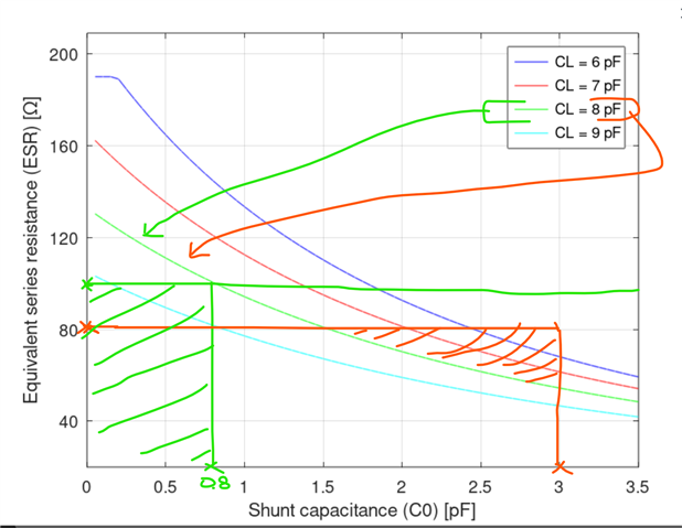
There is a graph in nRF54LM20 datasheet for crystal selection, a good candidate for crystal is the one that the rectangle from ESR value and shunt capacitance (C0) falls well below C_ line. The crystals you used, one of them is having area above CL line that might cause issue if the crystal fall in that region. The other one does not provide C0 value in datasheet, so we cannot fully conclude on that. In below picture green and red lines are two crystals you shared:
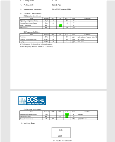
As as example below crystal would be a good candidate:
ECS-320-CDX-2152
Also please try to modify the USB VBUS pin path to make it similar to reference design to see if the issue persist or not.
Br,
Ressa
Generally speaking, discrepancies between the actual crystal used and the required specifications will result in frequency deviation, but will not completely prevent the crystal from oscillating. Furthermore, the crystal oscillates normally under Vbus power input. Based on common reasoning, the root‑cause of the issue lies not in the crystal oscillation circuit, but in different configuration settings adopted by the firmware for the applied components.We have checked the VBUS path and found no particular discrepancy versus the reference design
Only parameter that can have big impact on oscillation of crystal is internal load caps. Let me know what caps values you have used in FW for the mentioned crystals.
&hfxo {
load-capacitors = "internal";
load-capacitance-femtofarad = <8000>;
};