This post is older than 2 years and might not be relevant anymore
More Info: Consider searching for newer posts

feed line width for NRF52832 custom board

Hello, I am designing a PCB with NRf52832 IC. I have a query regarding the width of the feed line. In reference design files, the width of the feed line is 30mil. I have calculated the feed line with to match to 50-ohm impedance using an online calculator. Link of the calculator: emclab.mst.edu/.../index.html

My inputs for this calculator are:

H (Dielectric thickness) : 1.6mm

T (Trace thickness): 0.04mm (Got this value from PCB manufacturer)

εr (Relative permittivity): 4.7

Zo (Characteristic impedance): 50ohm

Output is W (Trace width) : 2.84mm Should I go with reference feed line width(30mils) or should I change the width a/c to this calculator(2.84mm)?

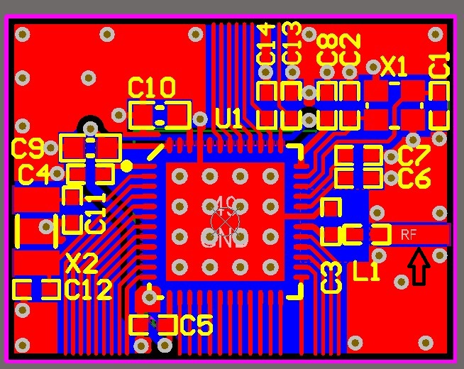
I have shown the feed line with arrow mark in below figure: image description

  • Hello Sweety

    The calculator you have used is for a transmission line type waveguide, with no ground plane on the layer where the conductor is placed. On the reference design there is a ground plane on each side of the conductor, in addition to the ground plane on the bottom layer. You therefore need to treat this as a co-planar waveguide with a bottom ground plane.

    Different calculators will give different results as they use different versions of the equations for calculating the impedance so only use the results as guidance. If you want to be completely sure you can make a small prototype PCB and measure it with a VNA.

    Using the Saturn PCB design toolkit to calculate the characteristic impedance of a coplanar waveguide with the parameters from the reference design (Trace width = 0,762mm, Substrate thickness = 1,6mm and conductor gap = 0,128mm) gives roughly 51,5 Ohms. This does give a slight mismatch but it should be fine, especially for short trace lengths. Do note that conductor thickness is not included in this calculator due to restrictions in the formula used, this seems to be quite common for most calculators. Using the same tool, your parameters gives roughly 32 Ohm characteristic impedance, which would cause a large mismatch for relatively short conductor lengths.

    Based on this I would recommend you stick to the reference design, or re-calculate your design parameters as a coplanar waveguide.

    Best regards

    Jørn Frøysa

  • Hello jorn, Thank you so much for the answer. I didn't understand the term " Conductor gap(0.128mm)". What does it mean?

  • The conductor gap is the gap between the conductor and the ground plane on the same layer as the conductor. It affects the capacitance of the conductor trace.

Related