This post is older than 2 years and might not be relevant anymore
More Info: Consider searching for newer posts

nrf8001 antenna feed width

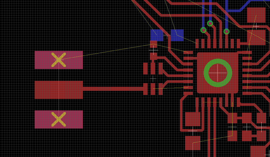
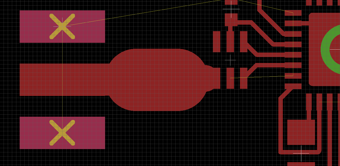
I am using the Johanson balun (www.johansontechnology.com/.../Johanson_nRF8001_App_Note_v2.pdf) to interface the differential input of the nRF8001. The PCB manufacture I am using is OshPark, which offers a FR408 with dielectric constant of 3.66. Because of this, my antenna feed line is only 13.5 mils thick to match 50 ohms.

Because of the smaller antenna feed line width, there are sharp right angles connecting from the SMA pad to the balun pad. Is this something I should be concerned about? Should I attempt to smooth the trace to the SMA/balun pad?

Also, should I care about the length of the feed line? I always thought the length of the feed line does not matter for the impedance matching, however I would like to clarify.

Thanks

I have attached an image of the feed line.

image description

  • Hi,

    First off you will have more losses in your line the thinner it is. In general we only require that the trace is 50 Ohm, however there are multiple ways to achieve this in a multilayer board. The width of the trace will increase with the thickness of the substrate.

    For reference the FR408 spec for OSHpark can be found in this link. If we use the upper layer as trace and the first conductive layer as ground we get a substrate thickness of 6.7 mil and a trace width of approximately 12 mil. However if we use the second conductive layer as ground we get a substrate thickness of approximately 53.7 mil and a trace width of around 108 mil. NOTE: These are rough calculations, and the values should not be used indiscriminately. A third option is using top to bottom for an even wider trace.

    If you do decide to use the thinner trace you will have to taper the line to match the SMA solder pad.

    The length of the feedline does not impact matching, however the length of the feedline is proportional to loss, so keep the lines short (particularly if they are thin).

    Best regards,

    Øyvind

  • By utilizing a bottom ground plane, I calculated the trace width to be 117 mil. I cannot find how to taper the antenna feed in eagle so I ended up routing multiple traces to perform "taper". Do you see there being an issue with the taper? Alternatively I might be able to do a copper pour and taper the polygon.

    image description

  • I am a little concerned about my calculations of line width. If I use the ground layer (3rd layer), then there are two dielectrics between the ground plane and the feed line. Is it safe to simply use the 3.66 dielectric constant even though the dielectrics are stacked?

    Thanks

  • Hi,

    After thinking a bit more on this I instead recommend that you use a coplanar waveguide. Calculators are available online, make sure that you use one that includes ground plane. The coplanar waveguide will be a lot easier to work with, sorry for the confusion.

    When you use a coplanar waveguide you can set the trace width to the width of the solder pad for the SMA connector, the impedance will depend on the gap between center trace and ground on each side. With a dielectric thickness of 6.7 mil I get much nicer values this was.

    Best regards,

    Øyvind

  • Thanks for the advice! That seems like a better solution. I'll check back in once implemented.

Related