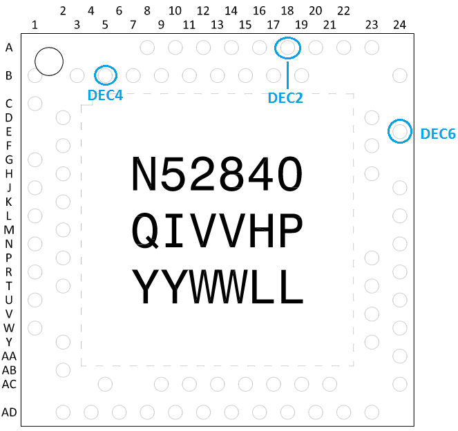
After the release of nRF52840 Engineering B we have received several inquiries about the difference between Engineering A (nRF52840-QIAAAA) and Engineering B (nRF52840-QIAABB) reference designs. One reason for the inquiries is that after swapping Engineering A with Engineering B samples customers experienced that the radio stopped working. The symptoms being that everything but the radio seemed to work in their application.
While this is highly unfortunate, it is to be expected because there was a vital design change in Engineering B. In Engineering A the two DEC2 pins (pin E24 and A18) and the DEC4 pin (pin B5) were internally connected within the SoC as shown in Figure 1 below (the two DEC2 pins belong in what the architects call the "same domain" which is why they share the same name). These three pins are used to decouple the 1.3V voltage regulator that supplies the radio. However, the radio architects struggled with noise and stability issues and traced the cause back to the internal connection. Their solution was to cut the internal connection in Engineering B. The cut was made at the green line shown in Figure 1, but this would require that the two pins are connected externally instead as shown in Figure 2.
This is one of the reference designs for Engineering A as shown in OPS v0.5.0:
Figure 1: Schematic for Engineering A as shown in OPS v0.5.0.
This is the equivalent reference design for Engineering B as shown in OPS v0.5.1:
Figure 2: Schematic for Engineering B as shown in OPS v0.5.1. Notice that the DEC pin at E24 has changed name to DEC6.
It follows that without neither an internal nor an external connection the radio will no longer work. Hence, PCBs designed for Engineering A samples will not work with Engineering B.
You might wonder why we connect DEC6 to DEC4 instead of DEC2 which is closer to DEC6 as is seen in the pin assignment in Figure 3 below. The reason is simply that this is what the architects found to give the best performance.

Figure 3: nRF52840 QIAABB pin assignment, top view.
As a side note, you might also notice that in designs using the DC/DC converter in Regulator 1 (REG1, Figure 2), there is an extra capacitor called C16 in parallel with C15, but this is not as critical as the external connection.
We normally publish Product Change Notifications (PCN) whenever a new SoC version is released. However, engineering samples are subject to frequent design changes and the Objective Product Specification (OPS) and reference designs might be changed without further notice. Changes will only be announced in the SoC's Revision history. So to avoid issues like these in the future:
- Always read the revision history when upgrading SoC. While the issues with the decoupling capacitors are not explicitly mentioned, there is indeed a sentence about changes made to reference schematics at the bottom of the list.
- Always read the updated errata list. While ideally each new revision should be less flawed than its predecessor, it is not uncommon that new errata are introduced in new SoCs. Therefore, it is crucial to always stay updated on the list and whether there are new pitfalls that might be relevant for your application.
- Always read through all the compatibility matrices. As bugs are fixed and features improved we usually release new SDKs and Softdevices taking advantage of this. New SDKs might not be compatible with old SoC revisions and vice versa.
Relevant reports in devzone:


Top Comments