

1.1 Description
This documentation describes the use and initialization of the Serial Wire Debug Port (SWDP) interface when writing to or reading from Flash and SRAM of the nRF52832 Rev 1. See http://infocenter.nordicsemi.com/ for more information on the IC itself.
DISCLAIMER: Not all content of this document has been verified and hence there might be some errors and flaws in the descriptions/information that follows. Please confer with the official ARM documentation to verify the information as described here. This information is provided in order to help during the implementation of a SWD debugger, but the official ARM documentation should still be used when doing so. Please contact us if you see any errors or flaws in the document so that it can be corrected. Also, if there are additions that would make sense to share or add, please send it to us for review.
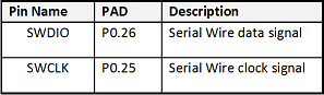
##1.2 SWDP Overall Specification## SWD (Serial Wire Debug) can be used to interface all memory locations of an nRF52832 device, including Flash and SRAM data. The interface requires two pins (in addition to power) according to the following table (please note that the SWCLK is sometimes referred to as SWDCLK in our documentation and other places):
###1.2.1 Debug Components in nRF52 ### The nRF52832 includes a SWD-DP (Debug Port), and a MEM-AP (Access Point). In addition to the default access port (AHB-AP), the DAP includes a custom Control Access Port (CTRL-AP) which, among other things, can be used to unlock the device if access port protection has been enabled. See the product specification for more details.
The maximum verified SWD speed on the nRF52832 is 8MHz. Faster speeds should be fine to use, but make sure to verify it is working before using these speeds in a production setup. The speeds might be limited by your PCB design or the traces used for the SWD communication, as well as the IC itself.
2 SWD in short
The SWDIO is bi-directional; meaning both the host (external debugger/test equipment) and the target (the nRF52832 device) can drive it. SWCLK is an input to the target, and must be driven by the host.
2.1 Clocking
The target drives and samples data on the positive edge of SWCLK. The host should therefore drive and sample the line in the space between the last negative edge and the next positive edge of SWCLK.
2.1.1 Host driving the data on the previous negative edge and sampling just before the next positive edge
This is considered the safest solution. In this case, the host can sample the data just before the next positive edge, since the host drives the clock.
Note that this solution may limit the higher SWD clock speeds if there are larger hold and setup time in the target. But this does not seem to be a problem with clock speeds up to 10MHz, see the product specification for the device to find the SWDP timing parameters.
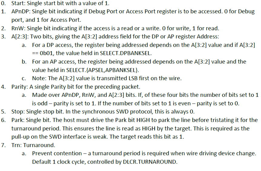
2.1.2 Packet Structure
An SWD packet consists of three parts: command, acknowledgement, and data. The host always sends the command, and the target sends acknowledgement. Either the host or target, depending on whether the command is a write or a read, drives data.
Whenever the SWDIO line changes driver, one “turn-around (Trn)” clock period is needed.
Below is an image (Made with wavedrom, .json attached) describing a write and read operation. Note the positions of the turn-around periods, and the parity bit at the end of the data word.

2.1.3 Command Structure
The command consists of the following 8 bits; see ARM Debug Interface Spec for more information:
2.1.3.1 DP/AP Registers
To make sense of the commands one needs to know where and what is written or read. A command is targeting either the Debug Port or the Access Port, which is defined by the APnDP bit as mentioned earlier.
Accessing the DP: When accessing the DP, the DP has certain registers that are of interest. The address of the access is as seen only submitted using two bits of the actual address. The rest of the address A[1:0] is defined by the SELECT register of the DP. By setting the last 4 LSBs of the SELECT register, you can define the DPBANKSEL, which defines the rest of the address not sent in the command. After powerup reset, this field is set to 0. For the nRF52832, DPv1 (see definition of DPIDR register and its value) is implemented, hence setting the DPBANKSEL means selecting which register you are accessing when reading/writing DP register at address 0x4.
DP address map:
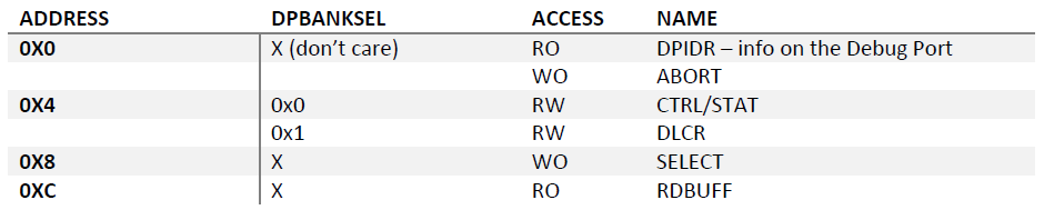
DPIDR will be value 0x2BA01477 for the nRF52832.
Accessing the AP: When accessing the AP, the AP has certain register that are of interest. The address is the same as for the DP access, and the APBANKSEL is also set through the DP.SELECT register. Another important note is that the SELECT register also defines which AP that is interfaced towards through its APSEL bits[31:24]. After a powerup reset, the value of this field is UNKNOWN which is why it should be set during the initialization sequence as described below. For the nRF52832, there are 2 APs, one is the normal memory access AP, and the other is the CTRL-AP. The normal AHB-AP is located at index zero, and our own CTRL-AP is at index 1, please see product specification for more information on this.
AP address map (please see ARM doc for the complete overview):
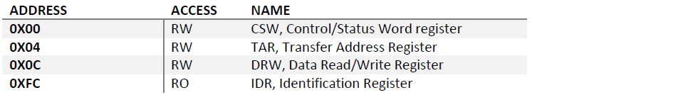
The CSW register configures and controls the access through the MEM-AP, such as the Size of the access and address auto-increment. The TAR register holds the address to be accessed, and the DRW register maps an AP access directly to one or more memory accesses. The CTRL-AP will have an IDR register of 0x02880000, and the normal AP will have the value of 0x24770011. This can be used to verify which AP one is connected to.
2.1.4 Acknowledgement Structure
Explanation of ACK structure. 001 OK, 010 Wait, 100 Fault (, 111 Protocol error).
The acknowledgement consists of the following 3 bits, see ARM Debug Interface Spec for more information:
ACK[0:2] – A three-bit target-to-host response, transmitted LSB first.
ACK responses (ref. section 4.3.2 ARM Debug Interface Spec (Successful write operation (OK response), 4.3.3, 4.3.4, 4.3.5):
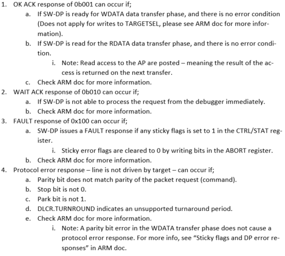
When in protocol error state, if the target detects a valid read of the DP DPIDR register, it is implementation dependent whether the target leaves the protocol error state, and gives an OK response. If the target detects a valid packet header, other than DPIDR register read, or detects an implementation-defined number of additional protocol errors, it enters lockout state.
Target must leave protocol error state/lockout state on a line reset. To be on the safe side, always perform a line reset if protocol error state or lockout state occurs with the nRF52832.
Host response to protocol error: If an unexpected response is received from the target, it must leave the line not driven for at least the length of any potential data phase, and then attempt a line reset.
2.1.5 Data Structure
Data is transmitted LSB first on the wire, both when writing (WDATA) and reading (RDATA). The parity bit on the data transfer is determined as following: The parity check is made over the 32 data bits, if the number of bits set to 1 is odd – parity is set to 1. If the number of bits set to 1 is even – parity is set to 0.
2.1.6 Turn Round
Line turn-round period is present to prevent contention. Required when device driving the wire changes, and is determined by DLCR.TURNROUND. Default is one clock cycle where neither host nor target drives the wire.
2.1.7 Idle cycles
An idle cycle is where the host clocks the SWD interface with the line LOW. After a transaction is completed, the host must either insert idle cycles, or continue immediately with the start bit of a new transaction, ref. 4.2.3 in ARM Debug Interface Spec.
3 nRF52832 SWD Setup and Control
This section will describe common use-cases of SWD access for the nRF52832. All use-case commands are describe in the following format: (COMMAND DATA, Comment). The data part will either be data transmitted by the host, or the data received from the target.
Unless otherwise noted; The BANKSEL of the commands is assumed not altered, meaning it is set to 0.
3.1 Initialization (Nordic specific entries)
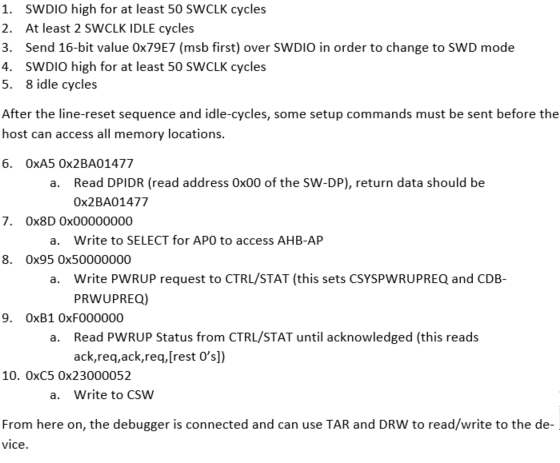
The SWD interface must be initialized by a “line-reset” sequence. For the nRF52832, this is defined as 50 SWCLK cycles with SWDIO driven high by the host. In addition, at least one idle cycle (SWDIO low) is required by ARM to let the DP exit reset state.
The initialization sequence can be summarized as following (for command explanation, please see below):
3.1.1 In depth explanation of the above sequence
Step 3 is required to switch from JTAG to SWD operation. Although the nRF52832 does not include any JTAG Debug Port, this command is still required to ensure that SWD communication is. Please see section 5.2.1 in ARM Debug Interface Spec for more information.
Step 6; Reading the DPIDR is recommended to make sure you are connected properly before you send commands. To describe the command 0xA5 0x2BA01477, the first part, 0xA5 (0b1010 0101) is the command itself, and the value that follows if the data part, which in this case is the value of the ID register returned by the nRF52832. The command 0xA5 is: Start(1),APnDP(0 – DP access),RnW(1 – read),A2:3,Parity(1),Stop(0),Park(1). The address read here is address 0x0, as SELECT is reset to 0 on powerup reset. DP register at address 0x0 is DPIDR which will return 0x2BA01477 for the nRF52832.
Step 7; Writing to SELECT in order to choose AP0, and not the CTRL-AP. Command: 0x8D (0b1000 1101 – DP, Write, Address 0b1000 – 0x8 – SELECT. Write value 0x00000000 – meaning we select AP 0 with no BANKSEL.
Step 8 and 9; Write PWRUP request of the debug system on device, and then wait for the request to be acknowledged.
Step 10; Write to CSW, value 0x23000052. These bits set some implementation defined values such as Bus Access Protection control. The whole value should be written to CSW. The lower 0x52 part specifies use of Auto increment, 32bit access, and device enabled for MEM-AP transactions.
3.2 Exit Debug Mode
In order to exit debug mode, write the following command with DP.SELECT address bank set to 0:
0x95 0x00000000 // Clear PWRUP Request to CTRL/STAT
The first part, 0x95, is the command sent by the host. What this command says is the following: 0x95 is the same as 0xb1001 0101. From the command description above, you can see that this translates into: Start(1), APnDP(0 – Debug Port), RnW(0 – write), A2:3, Parity(1), Stop(0), Park(1). This means, write to Debug Port, address 0b0100, the value that follows which is 0x00000000. The address is then defined by the DPBANKSEL register – which should be 0 for the exit debug mode command. Address 0x0100 (0x4 of the DP) is as seen above the CTRL/STAT register. Writing 0x0 to this register will clear all Debug resource requests and thus exit Debug Mode.
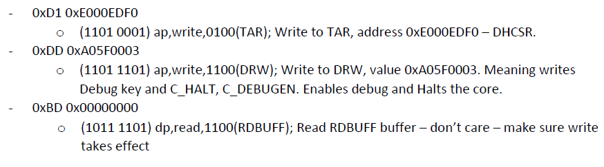
3.3 Halt Procedure
To halt the CPU, the following commands should work (these commands are explained in a slighty different way than earlier with the hopes that if you didn’t understand the earlier approach, this will make more sense. The bits of the command are listed in (…), along with an explanation of what the commands does below the commands themselves):
3.4 CPU System Reset hold and run
This sequence describes how to do a system reset with hold, then run.
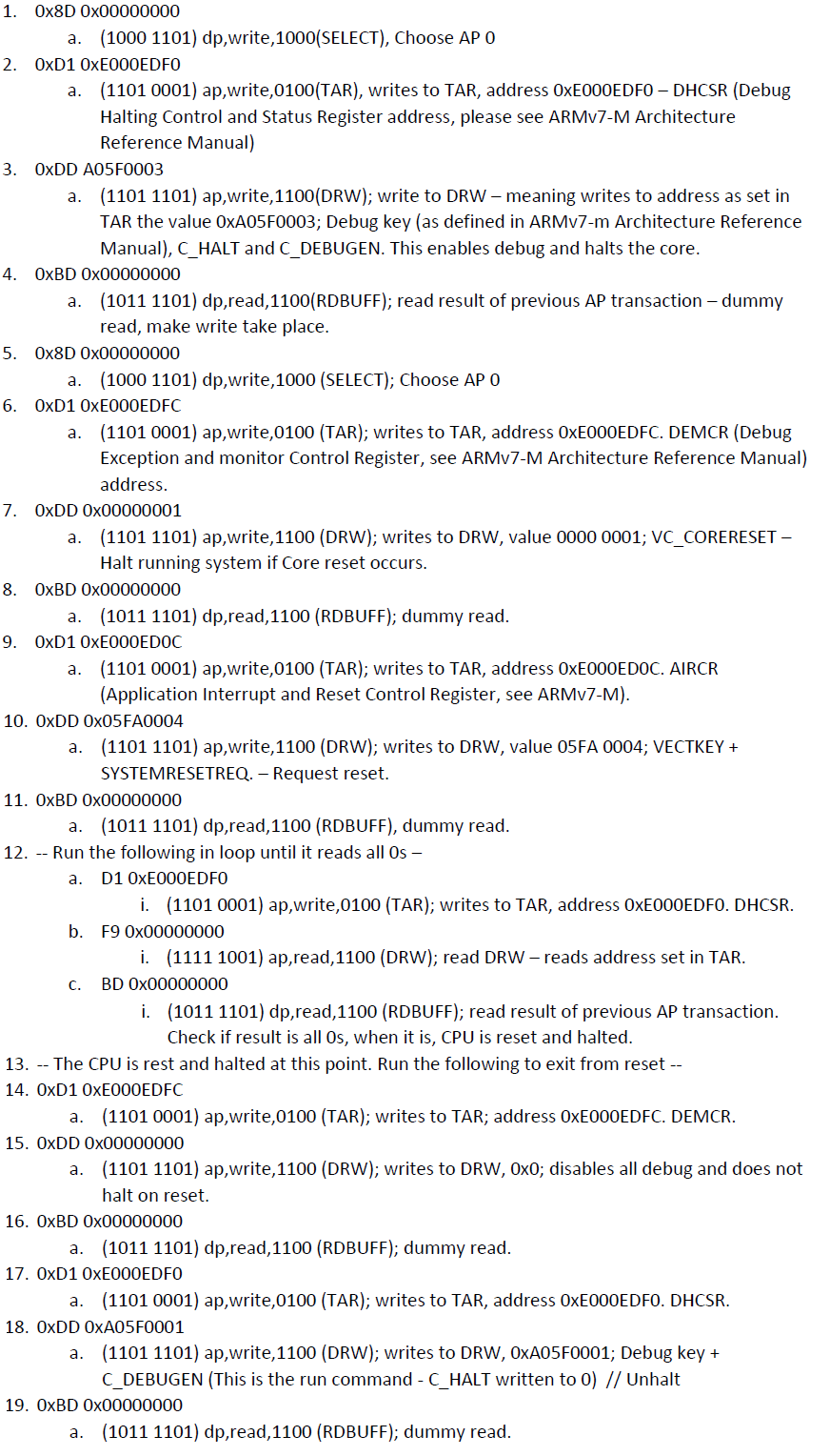
3.5 Execute from RAM
This sequence describes how to do execute from RAM, which may be useful if you are making a bootloader for example copying content into Flash.
In order to run program from SRAM the following commands are needed in order to set up the program counter and stack pointer. The processor must be halted before doing this. This approach assumes the program to be run is already in-place (programmed) in SRAM, and the program counter and stack pointer for your application needs to be known. Note: If you are flashing a .hex file, the stack pointer address is stored in the first word, and the program counter is stored at the second word.
To transfer a data word to an ARM core register, please see the ARM documentation. Basic approach; write to DCRDR which value. Write to DCRSR which register to write value.
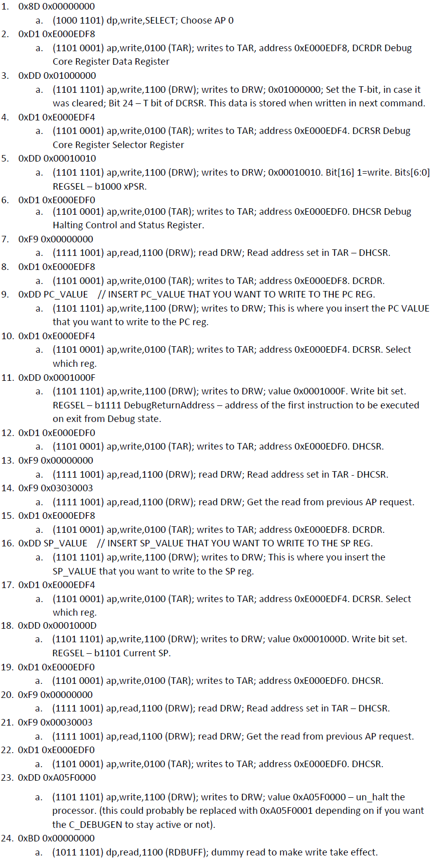
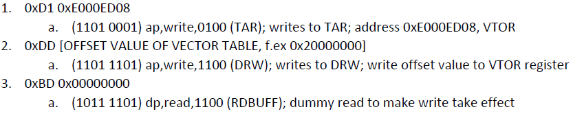
In addition to the sequence “Execute from RAM” above, if the vector table is needed because interrupts are being utilized; the following approach may be used to define the table vector offset for the core. Please see reference of VTOR register in the ARMv7-M Arch. Ref. Manual. VTOR is defined at address 0xE000ED08, and the [31:7] bits of this register define the TBLOFF, which are bits[31:7] of the vector table address used by the core. All the bits of the Vector table address that are not defined by the VTOR are zero. The VTOR register should be written before unhalting the processor, after having written the PC and SP registers.
To write VTOR, execute the following SWD commands:
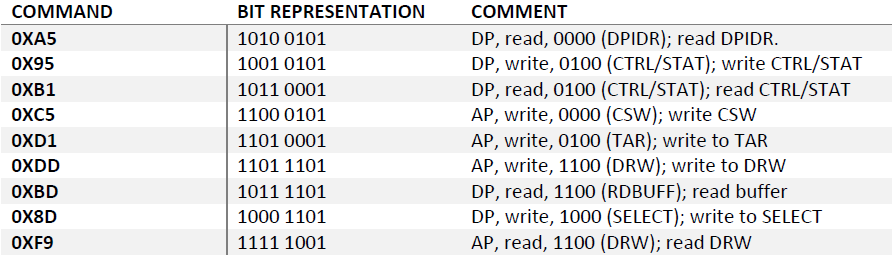
3.6 SWD Commands Bit Representation
The SWD commands are easier interpreted when translate into their respective bit-representations. The following table shows some of the commands used in this document and describes how they are interpreted with respects to the command structure as previously explained.
4 Example using JLink Commander
This section will describe how you can verify/test some of the functionality described here using the JLink Commander (JLink.exe) and a nRF52832-DK.
These tests were performed using SEGGER J-Link Commander V6.12a, and a nRF52832 (PCA10040) v0.9.0. To open the JLink Commander, simply double click the JLink.exe in the installed SEGGER software directory (C:\Program Files (x86)\SEGGER\JLink_V612a\JLink.exe), or type Commander in Windows Search and it should appear. For a Linux/OSX approach, I am hoping someone can test it and post their approach in the comments section below, or preferably send it to me, and then I will include it in this documentation.
4.1 Reading DPIDR
Testing DPIDR of the DP (address 0x0 in the DP) and checking if it matches the value 0x2BA01477 for the nRF52832.
Type "connect" to establish a target connection, '?' for help
J-Link>connect
Please specify device / core. <Default>: NRF52832_XXAA
Type '?' for selection dialog
Device>NRF52832_XXAA
Please specify target interface:
  J) JTAG (Default)
  S) SWD
TIF>s
Specify target interface speed [kHz]. <Default>: 4000 kHz
Speed>
Device "NRF52832_XXAA" selected.


Found SWD-DP with ID 0x2BA01477
Found SWD-DP with ID 0x2BA01477
AP-IDR: 0x24770011, Type: AHB-AP
Found Cortex-M4 r0p1, Little endian.
FPUnit: 6 code (BP) slots and 2 literal slots
CoreSight components:
ROMTbl 0 @ E00FF000
ROMTbl 0 [0]: FFF0F000, CID: B105E00D, PID: 000BB00C SCS
ROMTbl 0 [1]: FFF02000, CID: B105E00D, PID: 003BB002 DWT
ROMTbl 0 [2]: FFF03000, CID: B105E00D, PID: 002BB003 FPB
ROMTbl 0 [3]: FFF01000, CID: B105E00D, PID: 003BB001 ITM
ROMTbl 0 [4]: FFF41000, CID: B105900D, PID: 000BB9A1 TPIU
ROMTbl 0 [5]: FFF42000, CID: B105900D, PID: 000BB925 ETM
Cortex-M4 identified.
J-Link>swdselect
Select SWD by sending SWD switching sequence.
Found SWD-DP with ID 0x2BA01477
J-Link>swdreaddp 0
Read DP register 0 = 0x2BA01477
J-Link>exit
As you can see, the JLink commander already reads the DPIDR before it was done manually as part of the initialization sequence when choosing SWD. The result matches the expected values.
4.2 Reading Identification Register (IDR) of APs
On the nRF52832, there are two APs that can be accessed; the normal one, and the special CTRL-AP. This section will show how to read the IDR of these two APs. The IDR of the normal one should be 0x24770011, and the IDR of the CTRL-AP should be 0x02880000.
SAME SETUP AS EARLIER – connect, swd, etc…
…
J-Link>swdselect
Select SWD by sending SWD switching sequence.
Found SWD-DP with ID 0x2BA01477

// After initializing the SWD, you need to set the CDBPWRUPREQ and CSYSPWRUPREQ bits in
the SW-DP’s CTRL/STAT register. The command below writes the hex value into DP register 4 as
the bottom two bits are fixed. Regindex 1 gives (0b100) – 4.

J-Link>SWDWriteDP 1 0x50000000
Write DP register 1 = 0x50000000

// As the address field of the command is only two bits, you need to set the SELECT.APBANKSEL
(bits[7:4] of SELECT) in order to read the IDR register at 0xFC (0b1111 1100). Select register is
0x8 (0b1000) of the DP, so SWDWriteDP 2 – (0b10) does it. Writing the value 0x000000F0 sets the
APSEL to 0x00, and APBANKSEL to 0xF. We can then read the IDR of AP 0 in the next command
by reading 3 (0b11) which gives address (0b1111 1100 – 0xFC). The read has to be done twice
because the result of a read is return on the next AP access.

J-Link>SWDWriteDP 2 0x000000F0
Write DP register 2 = 0x000000F0
J-Link>SWDReadAP 3
Read AP register 3 = 0x00000000
J-Link>SWDReadAP 3
Read AP register 3 = 0x24770011

// Now to read the IDR of the other AP (CTRL-AP), we need to change the APSEL to 0x1. The
new read can then be done by the following commands. NOTE: As you can see, the read still
returns the result of the previous command for the first read, and the actual (new) result on
the next one.

J-Link>SWDWriteDP 2 0x010000F0
Write DP register 2 = 0x010000F0
J-Link>SWDReadAP 3
Read AP register 3 = 0x24770011
J-Link>SWDReadAP 3
Read AP register 3 = 0x02880000`
4.3 Halting the CPU
Following the procedure as mentioned earlier, the CPU is halted by writing to the DHCSR register.
SAME SETUP AS EARLIER – connect, swd, etc…
…
J-Link>swdselect
Select SWD by sending SWD switching sequence.
Found SWD-DP with ID 0x2BA01477
J-Link>SWDWriteDP 1 0x50000000
Write DP register 1 = 0x50000000

// From here on, the debug is up and running and TAR, DRW can be used to access memory

// First write the address of DHCSR into TAR

J-Link>SWDWriteAP 1 0xE000EDF0
Write AP register 1 = 0xE000EDF0

// Then write the value into DRW which will be written to DHCSR and halt the device

J-Link>SWDWriteAP 3 0xA05F0003
Write AP register 3 = 0xA05F0003

// Read RDBUFF and see if any errors in previous command

J-Link>SWDReadDP 3
Read DP register 3 = 0x00000000

J-Link>exit
The same thing can also be achieved by using the commanders “w4” command. The commander also takes care of most of the setup for you, so there should be no need to actually enable debug mode manually (it’s done automatically by the Commander). Hence, the same procedure can be done as following: “>connect”, “select SWD, nRF52 device and default speed”, “w4 0xE000EDF0 0xA05F0003”. This will halt the device.
5 References
- IHI0031C_ARM_debug_interface.pdf
-- This is the "ARM
 Debug Interface Architecture Specification ADIv5.0 to ADIv5.2” which can be downloaded from their website. You need to register as an ARM customer and download it from the following webpage: http://infocenter.arm.com/help/topic/com.arm.doc.ihi0031c/index.html
 - ARMv7-M Architecture Reference Manual –- You need to register as an ARM customer and download it from the following website: http://infocenter.arm.com/help/topic/com.arm.doc.ddi0403e.b/index.html
- nRF52832 Product Specification v1.3 -- http://infocenter.nordicsemi.com/ - nRF52 Series – nRF52832 – Product Specification

Top Comments