Hi there!
I am trying to set up external flash (w25q64) with my NRF52840 project over SPI. I have adapted the spi_flash sample in an attempt to set up this device, but I am having some issues that I think are related to the device tree. I can’t get the device to show as ready using device_is_ready(). Have I set something up incorrectly?
I’ve included my setup/wiring, prj.conf, overlay, and main.c.
NRF Connect SDK/Toolchain 2.5.1
Wiring:
| Module Pin | DK Pin |
| VCC | VCC |
| GND | GND |
| CS | P1.12 |
| MOSI/DI | P1.13 |
| MISO/DO | P1.14 |
| SCLK | P1.15 |
prj.conf
CONFIG_STDOUT_CONSOLE=y
CONFIG_FLASH=y
CONFIG_SPI=y
CONFIG_SPI_NOR=y
CONFIG_SPI_NOR_FLASH_LAYOUT_PAGE_SIZE=4096
nrf52840dk_nrf52840.overlay
&spi3_default {
group1 {
psels = <NRF_PSEL(SPIM_SCK, 1, 15)>, /* P1.15, D13 */
<NRF_PSEL(SPIM_MISO, 1, 14)>, /* P1.14, D12 */
<NRF_PSEL(SPIM_MOSI, 1, 13)>; /* P1.13, D11 */
};
};
&spi3_sleep {
group1 {
psels = <NRF_PSEL(SPIM_SCK, 1, 15)>, /* P1.15, D13 */
<NRF_PSEL(SPIM_MISO, 1, 14)>, /* P1.14, D12 */
<NRF_PSEL(SPIM_MOSI, 1, 13)>; /* P1.13, D11 */
low-power-enable;
};
};
&spi3 {
compatible = "nordic,nrf-spim";
status = "okay";
pinctrl-0 = <&spi3_default>;
pinctrl-1 = <&spi3_sleep>;
pinctrl-names = "default", "sleep";
cs-gpios = <&gpio1 12 GPIO_ACTIVE_LOW>; /* P1.12, D10 */
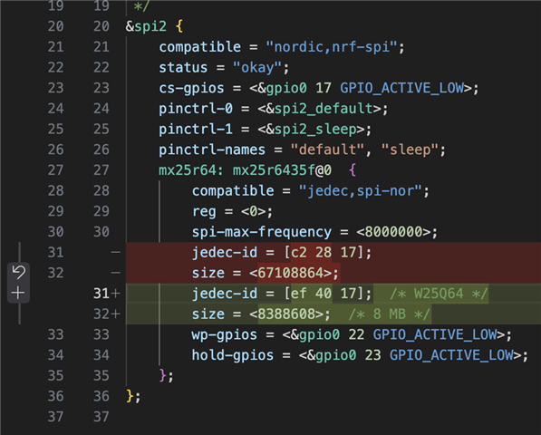
w25q64: w25q64@0 {
compatible = "jedec,spi-nor";
reg = <0>;
spi-max-frequency = <1000000>;
jedec-id = [ef 40 17];
size = <DT_SIZE_M(8)>;
};
};
&nrf_radio_fem_spi {
status = "disabled";
};
main.c
/*
* Copyright (c) 2016 Intel Corporation.
*
* SPDX-License-Identifier: Apache-2.0
*/
#include <zephyr/kernel.h>
#include <zephyr/drivers/flash.h>
#include <zephyr/drivers/spi.h>
#include <zephyr/drivers/gpio.h>
#include <zephyr/device.h>
#include <zephyr/devicetree.h>
#include <stdio.h>
#include <string.h>
#define SPI_FLASH_TEST_REGION_OFFSET 0xff000
#define SPI_FLASH_SECTOR_SIZE 4096
void single_sector_test(const struct device *flash_dev)
{
const uint8_t expected[] = { 0x55, 0xaa, 0x66, 0x99 };
const size_t len = sizeof(expected);
uint8_t buf[sizeof(expected)];
int rc;
printf("\nPerform test on single sector");
/* Write protection needs to be disabled before each write or
* erase, since the flash component turns on write protection
* automatically after completion of write and erase
* operations.
*/
printf("\nTest 1: Flash erase\n");
/* Full flash erase if SPI_FLASH_TEST_REGION_OFFSET = 0 and
* SPI_FLASH_SECTOR_SIZE = flash size
*/
rc = flash_erase(flash_dev, SPI_FLASH_TEST_REGION_OFFSET,
SPI_FLASH_SECTOR_SIZE);
if (rc != 0) {
printf("Flash erase failed! %d\n", rc);
} else {
printf("Flash erase succeeded!\n");
}
printf("\nTest 2: Flash write\n");
printf("Attempting to write %zu bytes\n", len);
rc = flash_write(flash_dev, SPI_FLASH_TEST_REGION_OFFSET, expected, len);
if (rc != 0) {
printf("Flash write failed! %d\n", rc);
return;
}
memset(buf, 0, len);
rc = flash_read(flash_dev, SPI_FLASH_TEST_REGION_OFFSET, buf, len);
if (rc != 0) {
printf("Flash read failed! %d\n", rc);
return;
}
if (memcmp(expected, buf, len) == 0) {
printf("Data read matches data written. Good!!\n");
} else {
const uint8_t *wp = expected;
const uint8_t *rp = buf;
const uint8_t *rpe = rp + len;
printf("Data read does not match data written!!\n");
while (rp < rpe) {
printf("%08x wrote %02x read %02x %s\n",
(uint32_t)(SPI_FLASH_TEST_REGION_OFFSET + (rp - buf)),
*wp, *rp, (*rp == *wp) ? "match" : "MISMATCH");
++rp;
++wp;
}
}
}
int main(void)
{
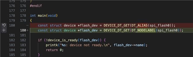
const struct device *flash_dev = DEVICE_DT_GET(DT_NODELABEL(w25q64));
for(int i = 0; i < 10; i++) {
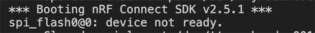
if (!device_is_ready(flash_dev)) {
printk("Attempt %u: %s: device not ready.\n", i + 1, flash_dev->name);
}
k_sleep(K_SECONDS(1));
}
if (!device_is_ready(flash_dev)) {
printk("Ending, %s: device not ready.\n", flash_dev->name);
return 0;
}
printf("\n%s SPI flash testing\n", flash_dev->name);
printf("==========================\n");
single_sector_test(flash_dev);
return 0;
}