This post is older than 2 years and might not be relevant anymore
More Info: Consider searching for newer posts

PCB - PCA10040's Stack-up question

Hi, I use the PCA10040 v1.1.
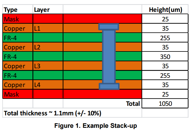
Example

This is an example of a PCB stack-up.

My questions are,

  1. In the case of PCA10040, which is 4 layered, what are the values of height in each layer?

  2. I'm creating a custom PCB using the nRF52832-QFAA.

However, due to cost, I'm going to make 2 layered, 1.6mm thick, FR-4 PCB.

The coplanar transmission line won't change even though I choose 2 layered PCB.

However, the height parameter of the stack-up seems to change.

If I create 2 layered PCB, what should be the height value to create a proper PCB?

-Best Regards

  • Hi, Bjørn. Yes, your assumption, set the thickness to 1.6mm, is correct.

    Can you explain more about the

    If this is just the substrate, i.e. the material inbetween
    the copper layers on the top and bottom,
    then you will have to subtract the thickness
    of those layers form (from typo) 1.6mm.
    

    I couldn't understand what you've meant.

    Lastly, about the picture of AppCAD that shows the parameters of the coplanar transmission,

    is the parameter L (length) is really 1000 mils (25.4 mm)?

    That looks quite long compared to the real PCA10040.

    -Best Regards

  • What I mean is that if L1( top copper layer) and L2( bottom copper layer) are 0.018 mm thick, then the thickness of the FR-4 substrate ( dielectric layer) between L1 and L2 must be set to 1.6 mm - 2*0.018mm = 1.56400mm. The L chosen in AppCad is just a random value, i.e. you will have to adjust this so that it matches your layout.

Related