This post is older than 2 years and might not be relevant anymore
More Info: Consider searching for newer posts

nrf52832 ble problem

I have designed nrf52832 customized board with tace antenna antenna and every pin of the controller is connected to the male headers present on both side of the boards. I havent used lpkf , so I changed the sdkconfig.h file to use internal RC but it wasnt working. By mistake , the P0.07 pin gets connected to Vcc and the led start blinking i.e. the bluetooth is advertising. Now ble is working fine but everytime I have to connect this P0.07 with 3.3v or also with little variation on that pin (like when I Just touch that pin with my fingers). I want to kmow that P0.07 is just an I/o pin , so why this behaviour? DOes it mean there is problem in my layout design.

There is no problem in the code as I'm using the standard code of ble of nrf52 dk by changing the sdkconfig.h as we dont have lpkf

  • Well broken ground plane seems to be your problem.

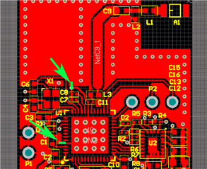
    As I show in the following image you have essentially isolated the ground of the nRF from the rest of the circuitry.  This is very, very bad.  It looks like the nRF might have a sliver of a ground connection at C7, C8 but even that is marginal.

    The way you have done the layout on your board none of the local capacitances are really doing anything since they are not connect to the same ground as the nRF.

    As to why it works when you hook up the gpio, some level of physics magic is happening.  Perhaps you are stabilizing the ground reference with that connection.

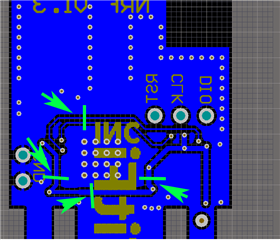
    For starters to prove to yourself that is the problem, solder some 30 gauge wires across your broken bottom layer in a few places and the problem should go away.  But you are going to have to redo your layout to fix it.

    I recommend you pass your updated layout by me for review when it is ready.

    Bridge the ground like this and see if it starts working.  Just scratch off some of the solder mask to connect the wires. Use really small gauge hookup wire, like 30 or 32 even 40 gauge is fine. On the Vss connection at pin 45 you can probably bridge it with a little dab of solder.  Just be careful not to short the pins.  If this connection scares you, then do the others first and see how it goes.

  • You don't have to do the connections precisely as I have shown, but you need at least 4 good connections around the chip to solve the problem and more connections is better.

  • Not sure why your cad app didn't pick up the mistake.  But the connecting dot at pin 49 is suspicious.  It's possible it didn't think the ground slug on the nRF was part of ground.

  • ohhh.. I see.. Thats a big mistake. The ground Pad of the nrf is connected through gnd just through cap C8 and C7 which is not sufficient, Thanku so much for pointing this out. I think this is the only problem.I will try to do the connections manually and for my new design checking that I will make, can I send the layout on your email id ([email protected]) or should I post it here ?

    and more thing. You said this

    "The way you have done the layout on your board none of the local capacitances are really doing anything since they are not connect to the same ground as the nRF."'

    because the nrf pad gnd is not at all connected to the gnd, its just through the c8 and c7. right?

  • You can send your updated layout for review to my email if you wish. 

    Yes the local capacitors are not doing anything because the length of board surface the current must flow is so long that there is significant resistive losses and parasitic inductance. Also since the ground currents for the entire nRF pass through that same narrow connection they talk to each other ( or couple). These are often called ground loops and are a large source of noise in a device.

Related