
Is there a way to have 6 different GPIOs act in unison off one event/action? I need all 6 to go ON and OFF at EXACTLY the same time based of an event or action.
Is there a way to have 6 different GPIOs act in unison off one event/action? I need all 6 to go ON and OFF at EXACTLY the same time based of an event or action.
A better way is to use a smaller FET to drive the larger one
Or to use a proper FET driver ...

the question still remains how to drive 6 outputs simultaneous.
I think the real question is, "how to drive the big FET?"
As noted above, trying to parallel 6 GPIOs is not a good answer to that question!
Hi,
I did some measurements by connecting a capacitor directly to one GPIO, then applying a 500 kHz pulse train.
390 pF, standard drive (S0S1 in NRF_GPIO->PIN_CNF):
390 pF, high drive (H0H1 in NRF_GPIO->PIN_CNF):

1000 pF, standard drive (S0S1 in NRF_GPIO->PIN_CNF):
1000 pF, high drive (H0H1 in NRF_GPIO->PIN_CNF):

Based on the above observations, it should not be a problem for a single GPIO to drive a 262 pF load at 400 kHz. The GPIO struggles a bit when driving 1 nF at 500 kHz, with standard drive strength, but still should be able to open/close a FET with this gate capacitance.
Here's the example I used for reference (copy it into the blinky example for instance):
/**
 * Copyright (c) 2014 - 2018, Nordic Semiconductor ASA
 *
 * All rights reserved.
 *
 * Redistribution and use in source and binary forms, with or without modification,
 * are permitted provided that the following conditions are met:
 *
 * 1. Redistributions of source code must retain the above copyright notice, this
 *    list of conditions and the following disclaimer.
 *
 * 2. Redistributions in binary form, except as embedded into a Nordic
 *    Semiconductor ASA integrated circuit in a product or a software update for
 *    such product, must reproduce the above copyright notice, this list of
 *    conditions and the following disclaimer in the documentation and/or other
 *    materials provided with the distribution.
 *
 * 3. Neither the name of Nordic Semiconductor ASA nor the names of its
 *    contributors may be used to endorse or promote products derived from this
 *    software without specific prior written permission.
 *
 * 4. This software, with or without modification, must only be used with a
 *    Nordic Semiconductor ASA integrated circuit.
 *
 * 5. Any software provided in binary form under this license must not be reverse
 *    engineered, decompiled, modified and/or disassembled.
 *
 * THIS SOFTWARE IS PROVIDED BY NORDIC SEMICONDUCTOR ASA "AS IS" AND ANY EXPRESS
 * OR IMPLIED WARRANTIES, INCLUDING, BUT NOT LIMITED TO, THE IMPLIED WARRANTIES
 * OF MERCHANTABILITY, NONINFRINGEMENT, AND FITNESS FOR A PARTICULAR PURPOSE ARE
 * DISCLAIMED. IN NO EVENT SHALL NORDIC SEMICONDUCTOR ASA OR CONTRIBUTORS BE
 * LIABLE FOR ANY DIRECT, INDIRECT, INCIDENTAL, SPECIAL, EXEMPLARY, OR
 * CONSEQUENTIAL DAMAGES (INCLUDING, BUT NOT LIMITED TO, PROCUREMENT OF SUBSTITUTE
 * GOODS OR SERVICES; LOSS OF USE, DATA, OR PROFITS; OR BUSINESS INTERRUPTION)
 * HOWEVER CAUSED AND ON ANY THEORY OF LIABILITY, WHETHER IN CONTRACT, STRICT
 * LIABILITY, OR TORT (INCLUDING NEGLIGENCE OR OTHERWISE) ARISING IN ANY WAY OUT
 * OF THE USE OF THIS SOFTWARE, EVEN IF ADVISED OF THE POSSIBILITY OF SUCH DAMAGE.
 *
 */
/** @file
 *
 * @defgroup blinky_example_main main.c
 * @{
 * @ingroup blinky_example
 * @brief Blinky Example Application main file.
 *
 * This file contains the source code for a sample application to blink LEDs.
 *
 */

#include <stdbool.h>
#include <stdint.h>
#include "nrf_delay.h"
#include "boards.h"

#define MY_PIN  3

/**
 * @brief Function for application main entry.
 */
int main(void)
{
    nrf_gpio_cfg_output(MY_PIN);
    NRF_GPIO->PIN_CNF[MY_PIN] |= GPIO_PIN_CNF_DRIVE_H0H1 << GPIO_PIN_CNF_DRIVE_Pos;
    NRF_CLOCK->TASKS_HFCLKSTART = 1;
    while (NRF_CLOCK->EVENTS_HFCLKSTARTED == 0)
    {
    }
    NRF_CLOCK->EVENTS_HFCLKSTARTED = 0;

    NRF_POWER->TASKS_CONSTLAT = 1;

    NRF_GPIOTE->CONFIG[0] = GPIOTE_CONFIG_MODE_Task << GPIOTE_CONFIG_MODE_Pos |
                            GPIOTE_CONFIG_POLARITY_Toggle << GPIOTE_CONFIG_POLARITY_Pos |
                            MY_PIN << GPIOTE_CONFIG_PSEL_Pos |
                            GPIOTE_CONFIG_OUTINIT_Low << GPIOTE_CONFIG_OUTINIT_Pos;

    // Set prescaler to 4, 1 us resolution
    NRF_TIMER1->PRESCALER = 4;

    NRF_TIMER1->BITMODE = TIMER_BITMODE_BITMODE_32Bit << TIMER_BITMODE_BITMODE_Pos;
    NRF_TIMER1->CC[0] = 1;
    NRF_TIMER1->SHORTS = TIMER_SHORTS_COMPARE0_CLEAR_Enabled << TIMER_SHORTS_COMPARE0_CLEAR_Pos;
    NRF_TIMER1->TASKS_START = 1;

    NRF_PPI->CH[0].EEP = (uint32_t) &NRF_TIMER1->EVENTS_COMPARE[0];
    NRF_PPI->CH[0].TEP = (uint32_t) &NRF_GPIOTE->TASKS_OUT[0];

    NRF_PPI->CHENSET = PPI_CHENSET_CH0_Enabled << PPI_CHENSET_CH0_Pos;
    /* Toggle LEDs. */
    while (true)
    {
        __WFE();
    }
}

/**
 *@}
 **/
Q1: Are you configuring your GPIO as High Drive in both directions (ie: setting NRF_GPIO->PIN_CNF[my_pin], field "DRIVE" to "H0H1")? This is very important that you set, as you will source and sink the input capacitor at the gate. If you set H0S1, the GPIO may have troubles driving the signal high.
Q2: Which 6 pins are connected together? For instance: The NFC pins on the nRF52832 (P0.09 and P0.10) need to be explicitly set to "normal GPIOs" in UICR if you use these.
Q3: Is it possible to test one GPIO "standalone", by physically disconnecting the other 5 GPIOs?
Q4: Do you see this issue on more than one board? Just to rule out if your current board has gotten any damage to one of the GPIOs connected in parallel.
Q5: If using a series resistor between the GPIO and the FET gate, this would also limit the rise-fall time. Could you test without having a series resistor?
Kind regards,
Håkon

In our initial circuit we had 6 GPIO from the Nordic nRF52832 driving the gate of an NFET thru a 33.2 ohm resistor. Here are the relevant parts of the schematic. We connected P0.05 thru P0.10 together to drive the NFET.
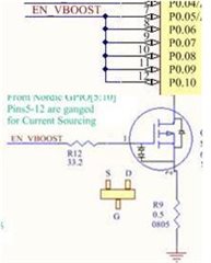
The intent was to drive all 6 pins from a single PWM channel so that all pins were in sync.
In the initial programming of the PWM it seemed easiest to define all 4 channels to individual GPIOs and to try driving the gate with 4 GPIO.
The NFET we designed in was Vishay/Siliconix SQ2364EES. This part was chosen because of its low RDSon
This part has an input capacitance of 330pf @25V
The 4 GPIO do not seem able to drive this NFET, it could be because of the input capacitance or something else unique to this chip. Here is an example of the drive at the gate.
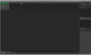
Here is a sample trace of the NFET gate (with no gate resistor or source resistor). This is directly out of the 4 Nordic GPIO pins. This signal is 50% duty cycle at 400khz.
Note that the high level of the GPIO never goes above .7V, and when it tries to bring it to ground is very slowly ramps to ground
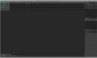
Similarly, here is the same 50% signal, with 4 outputs set to H0S1
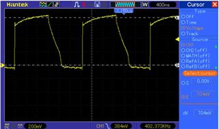
It should be noted that NEITHER of these signals is actual turning on the NFET in a way that our circuit works.
At this point we decided to try a different NFET that had a lower input capacitance:
Diodes Inc, DMN62D0U-13
This part has an input capacitance of 32pf @30V
The Nordic 4 GPIO seem to be able to drive this NFET.
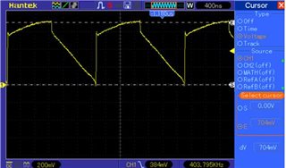
Here is a sample trace of the NFET gate (with 33.2 ohm gate resistor but no source resistor). This is the actual gate signal. This signal is 50% duty cycle at 400khz.
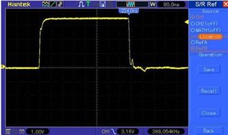
Note that this signal goes all the way up to 3V, and though the edges are not sharp it does allow our circuit to work.
We would rather use the initial NFET because of its low RDSon. The RDSon of the NFET has a significant impact on our circuit response. For some reason the Nordic seems unable to drive this chip. I don’t know that even 6 GPIO will be able to drive it.
To answer your questions (if the weren't answered above
1) I have tried driving the original FET at all variants of drive H0H1, H0S1, S0H1, S0S1
2) We connected P0.5 to P0.10, but using P0.5 to P0.8 with the PWM and putting P0.9 and P0.10 (NFC) as disconnected inputs. Also, obviously the pins work with the new FET so it is more an issue with the original FET
3) We cannot easily disconnect the pins. We did set them in software as disconnected inputs as a test
4) 3 of the original boards I tested they all act the same. It might be possible that our contract manufacturer put the wrong part on the board. I will pursue that by ordering new parts and replacing the existing one. As seen above, a different FET works just fine (even with one Nordic GPIO)

Thanks for the detailed answer. Given that you have tried this on 3 different boards, I believe we can rule out any damage to one of the 6 GPIOs.
I'm trying to source the specific FET that you're using locally, so I can redo the measurements on actual target.
The two devices you're testing with has the same pin out, according to their respective datasheets. However; It looks like there's something clamping your levels to ~0.7V in the first two scopes, which closely resembles a diode drop.
What is the marking on your device? According to the datasheet (below "Product Summary"), it should be 9Jxxx on the SOT-23 package. Could you check that your part has this marking?
Kind regards,
Håkon