Hello everyone,
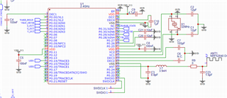
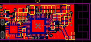
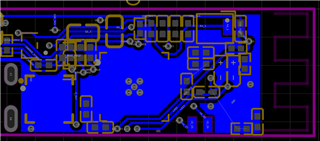
I created my first own layout design and the antenna. Before I order the PCB I hope you guys can review it one time. I tried to get the most informations from the forum, but I was not able to answer all of my questions. The PCB has a size of 12mm x 43mm and has only 2 layers, therefore I was not able to take over the reference layout. I tried to take over as much as possible from the reference layout of the NRF52832. I used the tool EasyEDA for designing the schematic and layout.
I never designed a antenna before and I tried to copy the design from the NRF52840 dongle. Which range can I expect from this antenna? I read alot regarding the 50Ohm Impedance, but i didnt completely get from where to where is the 50 Ohm. I know there is a matching circuit C3 and L1 the µC see a Impedance of 50 Ohm. Where I need to design the next 50Ohm from L1 to R9 or from L1 to end of the antenna?
Can you please give me a feedback if the device and antenna will work? And if not please give me a feedback what I could improve. If you need any additional information I will deliver them as fast as possible.
The Top Layer:
The Bottom Layer:
Schematic: