Hello Nordic team,
I am designing a 10-layer PCB with nRF52840.
Should I place a ground plane under the chip in each layer, connected through the vias in the middle ground pad? Or using few of the layers is enough?
Thanks,
Avihay
Hello Nordic team,
I am designing a 10-layer PCB with nRF52840.
Should I place a ground plane under the chip in each layer, connected through the vias in the middle ground pad? Or using few of the layers is enough?
Thanks,
Avihay
The best practice is to isolate the antenna area on every layer(not even ground planes). However, the GPIO area can "suffer" the presence of signals - you can take a look even at the DK schematics:
devzone.nordicsemi.com/.../custom-pcb---nordic-board-layout-spec-question
Hi Avihay,
Having ground under the SoC on all layers are not required. But there should be at least one continuous ground plane connected to the vias under the SoC that can act as the reference ground for the transmission line. In our reference design we use the bottom layer as the reference ground for the transmission line, but a inter layer can also be used. Keep in mind that the width of the transmission line is dependent on the distance to the ground layer beneath.
We have also seen some problems with designs where there is a VDD layer directly under the SoC, so I recommend to have a ground fill under the SoC on the 2nd layer.
We can do a review of your design, just create a private ticket and share your design files and one of our hardware engineers will give you feedback on it.
Best regards,
Bendik
Hi Bendik,
Thank you for your answer and thanks for the suggestion for the design review, for sure I will send it once it will be ready.
Thanks again,
Avihay
Hi Meh,
Thank you for your reply!
AvihayZ said:Can you share a rule of thumb for calculating the width of the transmission line?
A tool like AppCAD or Saturn PCB Toolkit can be used to calculate the impedance of the transmission line, which is directly dependent on the width of the trace. When using these tools its important to select the correct dielectric constant for the PCB substrate you are using, you can get this information from the PCB manufacturer you are using.
AvihayZ said:And regarding your remark of the VDD layer under the SoC - do you see any problem with having a VDD layer in the 5th layer, assuming:
- there is a GND fill under the SoC on the 2nd layer?
- there is a GND fill under the SoC on the 9th layer?
This shouldn't be a problem.
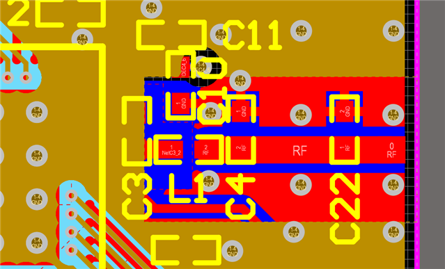
If you are using the 9th layer as the reference ground for the transmission line you will need a keep-out area under the transmission line on layers 2-8 like we have on the internal layers in the reference layout:

Best regards,
Bendik