This guide will cover the specific areas that must be paid extra attention to when designing a PCB for nRF52805. It is intended as a nRF52805 specific addition to the General PCB design guidelines for nRF52, which should be read and followed unless otherwise instructed in this blog post.
Reference design
The nRF52805 reference schematic illustrates the required and optional external passive components, as for all Nordic Semiconductor products.
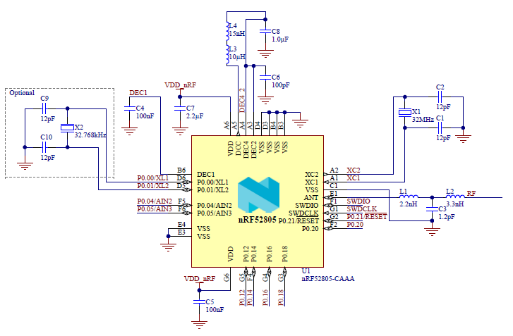
The reference design is available at the nRF52805 product page and can be imported directly to a specific design. If made from scratch it is important to make sure the schematic is replicated perfectly. Pay extra attention to the connection between DEC4 and DEC2, not connecting these together will degrade RF performance.
The reference layout should also be replicated as closely as possible. This is the PCB layout that is tested and verified by Nordic Semiconductor, deviating from it might alter performance.
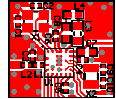
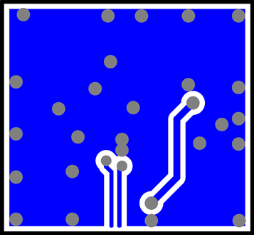
Note especially the position, connection and grounding of the capacitors on DEC2 and DEC4 (C6 and C8), if this is not replicated, RF performance might be degraded. The RF matching network (L2, C3 and L1) positioning and grounding is also important for good performance that is compliant with regulatory requirements.
PCB stackup.
Contrary to other nRF52 WLCSP devices, nRF52805 is optimized for a 2-layer PCB stackup. To enable this, it is however important that the bottom layer is a mostly solid ground plane to ensure a good ground connection for the IC. 2-layer stackups should also only be used with substrate thickness 0.7mm or less, to ensure good RF performance.
In designs that need the space underneath the nRF52805 for other components or trace routing, a 4 or more-layer stackup should be used, using at least one internal layer as ground plane.