
This guide will cover the specific areas that must be paid extra attention to when designing a PCB for nRF52832. It is intended as a nRF52832 specific addition to the General PCB design guidelines for nRF52, which should be read and followed unless otherwise instructed in this blog post.
Reference design
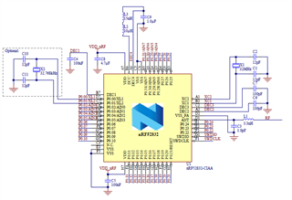
The nRF52832 reference schematic illustrates the required and optional external passive components, as for all Nordic Semiconductor products.
nRF52832 QFAA/QFAB reference schematic:
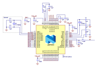
Note especially C13 and C14, these are a workaround for errata 138. An alternative workaround is to tie the PCB solder pads of P0.25 and P0.26 into the center pad of the IC, if the pins are not in use.
A key difference between the reference schematics for the QFN package variant and WLCSP reference designs is DEC2. DEC2 shall be decoupled with a 100pF capacitor in designs using the WLCSP variant, and not decoupled in designs using the QFN part.
nRF52832 CIAA reference schematic:
-

T IJ
-
Cancel
-
Vote Up
0
Vote Down
-
-
More
-
Cancel
-

JONATHAN LL
in reply to T IJ
-
Cancel
-
Vote Up
0
Vote Down
-
-
More
-
Cancel
Comment-

JONATHAN LL
in reply to T IJ
-
Cancel
-
Vote Up
0
Vote Down
-
-
More
-
Cancel
Children