This post is older than 2 years and might not be relevant anymore
More Info: Consider searching for newer posts
This discussion has been locked.
You can no longer post new replies to this discussion. If you have a question you can start a new discussion

Altering QSPI Address Mode?

I have recently acquired a NAND chip from Micron and would like to use it for storage.

However, looking through the datasheet I found out that the addressing scheme require by the Micron chip is a bit different from the QSPI used in the SoC.

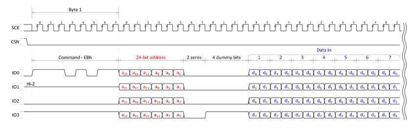
For READ, READ2O and READ4O, the pattern of the address bytes following the command byte are the same for the chip and the SoC, but for READ2IO and READ4IO, they are different.

SoC QSPI:

image description

Micron chip:

image description

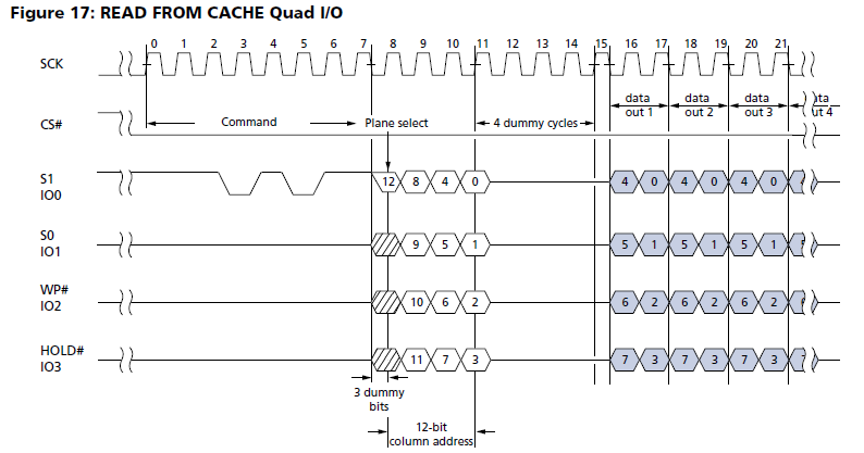
Notice how the address required by the Micron chip is only 12 bits + 3 dummy bits. The same behavior goes for the write as well.

Is there a way to overcome this so that I can use IO operation instead of O on the chip?

  • Hi Fan,

    Could you please provide the datasheet of the NAND flash ?

  • Hi, the datasheet actually require login in order to retrieve it from the Micron website. However, I manage to find a similar chip that has open access link. It differs from the chip that I am currently using but the addressing scheme is the same. Link: datasheet.octopart.com/MT29F1G01AAADDH4-IT:D-Micron-datasheet-11572380.pdf My main problem is that the chip has write issue because the address is 16 bits. (13 + 3 dummy bits, sorry for the error in the question)

  • Hi Fan,

    Could you point me to the figure/description showing the difference in addressing scheme in the new datasheet ? Now you are concerning write command not read command ?

  • I wanted to use multiple IO lines for read and write, after I post the question, I realize the difference in addressing scheme affects both the operations. For example Figure 13 and Figure 14 in the datasheet shows the addressing scheme using 16 bits. As for the write, Figure 16 also shows that (This 1Gb chip does not support more than one IO line for write, but for the one I am using, it has an additional write mode that uses 4 data lines to send data, which is the picture in my original question). But the problem is that the difference in the 24 bits and 16 bits addressing means I would loss data when reading and transfer wrong data when writing. To be more clear, for read, there is a work around in the chip that I am using but is not shown in the datasheet that I pasted (I am sorry for that), but the write has this addressing issue that I total cannot write correctly to the chip.

  • To add on, the onboard flash is capable of using 24 bits for the addressing, such as section 10-12, 10-14, 10-22, 10-23 in the datasheet: www.macronix.com/.../MX25R6435F, Wide Range, 64Mb, v1.4.pdf Although this is NOR and mine is NAND, I am not very sure does this means there is a difference in the NOR and NAND addressing schemes.

Related