This post is older than 2 years and might not be relevant anymore
More Info: Consider searching for newer posts

experimental ble blinky doesn't work

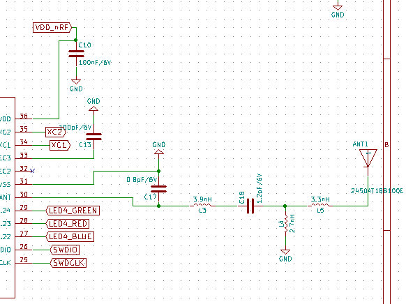
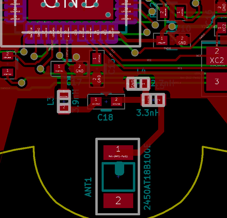
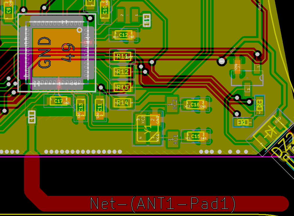
Hi everybody, I have an issue with my application, I use the nRF52832-QFAA with the following circuit, when I open the application Nordic 'nRF Connect', I detect the ble when I use the example from Nordic 'experimental ble blinky' with the devellopment board (PCA10040) but when I program my application with the Jtag I can't detect the device, I don't know if this issue come to the antenna, do you have an idea why it doesn't work ?

Thank you for your help image description image description

  • I forgot to precise that I use SDK13 and the SoftDevice 4.0.2 with nRFgoStudio

  • Hello Omar

    Your schematic seem to be in line with the reference circuits of both the nRF and the antenna. Have you remembered to include a 32MHz crystal?

    There are however some flaws in your layout that will need to be amended. From what I can see on the picture you posted you do not have a ground plane underneath the components and transmission lines, which make out your matching network. It also seems you have routed signal traces underneath parts of it (the green lines).

    High frequency systems are very sensitive to the physical layout, and any component/transmission line should have a whole, unbroken ground plane underneath. There should not be any traces or components underneath the traces and components which make out the matching network.

    Traces connecting the different components in the matching network should be kept as short as possible to minimize their impedance transformation. The line between the nRF matching network (C17 and L3 in your schematic) and the antenna matching network (C18, L4 and L5) can be of some length, as long as its properly designed with a characteristic impedance of 50 Ohm. In the area where the matching network is you should only have top and bottom layers, mid layers should be omitted.

    Please read the PCB guidelines stated in the nRF52832 product specification carefully. Also see this link for further guidelines.

    In the area surrounding the antenna you should maintain a keep-out region. No components, additional traces or copper planes should be placed within this region.

    As stated on page one of the antenna datasheet, there should be a ground plane perpendicular to the orientation of the chip-antenna. For the best performance please follow the layout instructions in the datasheet.

    Edit for additional answers

    When using a monopole PCB trace antenna you will need to tune the antenna by using a shunt capacitor close to the base of the antenna (but outside the keep-out region) in conjunction with trimming the antenna length (cutting the tip of the antenna). You have not included this capacitor in your design, I would recommend you include it as the antenna is quite likely to need matching. See this whitepaper for more information.

    The line between the shunt capacitor of the antenna, and the matching network of the nRF52 needs to be 50 Ohm as you've stated. The lines connecting the different components in the matching network needs to be as short as possible, and wide enough to handle the current present. The impedance at a given point within the matching network will be complex and any lines of significant length will cause phase shifts, which again causes mismatch. I recommend you follow the PCA10040 layout found in the DK hardware files. The lines connecting the matching network components seem a bit thin and long. You should make them as short as possible, and make sure they are wide enough to handle the current.

    Best regards

    Jørn Frøysa

  • I discovered that the Quartz is not well conneted. that can affect Bluetooth and make it not working !!

  • Thank you for your response Jorn, I noticed that I have an issue with the footprint of my 32MHz crystal, I think this is the problem. I have done it again without ceramic antenna but with the same antenna that the board devellopment Nordic nRF52832 PCA1004. I use Coplanar waveguide to get an impedance of 50 Ohms between the antenna and the first inductance, Is there a specification for the line between the inductance and the capacitor ?

    image description

    Do you think that this pcb is correct ?

    Thank you for your help

  • I have updated my original answer with additional information.

Related