Hi, We are designed our own Beacon PCB based on nRF51822 Beacon Kit...We followed board size,PCB Antenna Trace width and GND Clearance as per Beacon kit...The difference is NRF51 Package we followed QFN instead of BGA...
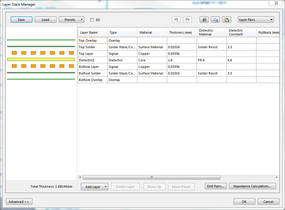
We have to include FAB details like Board Thickness,Material and Finish copper for making PCB...Also we need complete 2 layer Stack up as nRF51822 Beacon kit followed,so that we can achieve the antenna performance ( like 50 Ohm Impedance details)...
Currently we followed 1.6mm Board Thickness,FR4 material and 1 oz (35 Micron) finish copper and no information for 50 ohm Impedance....But we want make sure our data are correct to match the antenna to perform 100% like beacon kit...
Note: Its Exactly copied from beacon kit (Including GND and Trace width and all passives). Currently the board is in Fab house to wait for the above data...Kindly provide the required information...