This post is older than 2 years and might not be relevant anymore
More Info: Consider searching for newer posts
This discussion has been locked.
You can no longer post new replies to this discussion. If you have a question you can start a new discussion

Suggestion for Custom nRF52832 specially RF Antenna

Hello Sir,

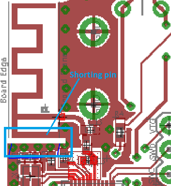
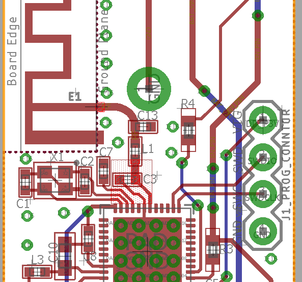
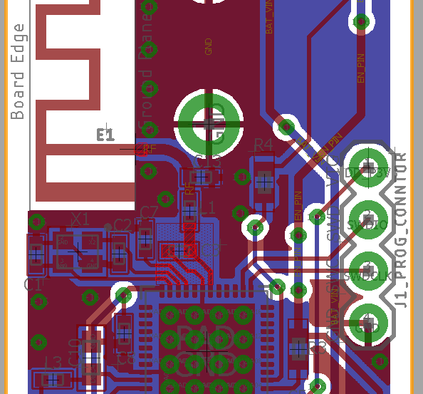
we have designed custom PCB using nRF52832, I am little confused for is it OK. I have attached top and bottom layer layout of my PCB please sir review it and is it ok like antenna and Specially for RF components placement. Give me your valuable suggestion for same we are planing to manufacture this PCB design for Vendor. Can also suggest me for board performance what is required PCB material for working nordic RF board. We need to tell that specification to my PCB manufacturer Vendor. Please give me your valuable suggestion. nRF52832_updated

Lyout_updated

Thanks in advanced.......!

  • Hi,

    First I'd like to point you to our reference designs, PCB guidelines and layout examples, and this PSB design post.

    1. We always recommend copying our reference design and layout.
    2. When working with 2.4 GHz signals, every millimeter of PCB trace is important. Traces should be as short as possible and components should be mounted as close to the nRF52 as possible. Your image is quite low resolution so I can't read all the component names, but the inductor in the matching network should ideally be placed a little closer to the SoC and so that the two traces from the VSS and ANT pins are equally long (refer to the reference layout).
    3. If you move the inductor it would also be possible to move the two DEC2 and DEC3 decoupling capacitors closer to their pins and hence shorten the traces (The DEC2 capacitor is marked as NC in the schematic for QFN packages and it is safe to remove it from your layout).

    EDIT 23.01.2018

    1. I have one more comment about your antenna design. To get the correct impedance in your shorting pin you need to remove some of the ground plane as shown in the image below:

    image

    Rearrange the crystal etc. as necessary to get adequate space for this. Unfortunately we don't have any documentation on proper design of inverted F antennas, but there should be plenty online.

  • Thanks sir, I have designed my schematic by using this reference design only due to some size matter i have little change of components placement on layout. As per your suggestion i remove DEC2 capacitor from my design and move nearest DEC3 cap to nRF52. And sir is it ok PCB antenna place and other components also for good RF performance. For better view my layout and schematic to you how i can upload in pdf format with this comment.

  • Hi, Please see my edit above.

    To insert images in your text you can do like this:

    1. Type in an image description where you want to place your image in the text.
    2. Click the insert image button
    3. Click "Choose file", and choose your file.
    4. Click OK.

    image description

  • Thanks for your quick reply, I have edited my layout as per you suggested me like remove some GND plane and rearrange crystal. i have attached my new images in above as a edited. Please sir review this let me know is it ok Can i go for PCB manufacturer and assemble this board. Thanks.........

  • You should have a little more room between your shorting pin and the ground plane. 5mm or more is ideal.

    BTW, you can also upload the gerber files in a zip file. That will make it easier to review.

Related