This post is older than 2 years and might not be relevant anymore
More Info: Consider searching for newer posts

Using Nrf51422 as I2C(TWI)

Hello

I have an problem using I2C on my custom board which uses an Nrf51422 SOC. I have an RTC chip connected to it and I have no idea how to use your libraries.

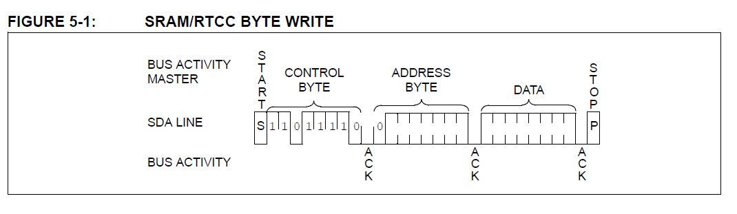
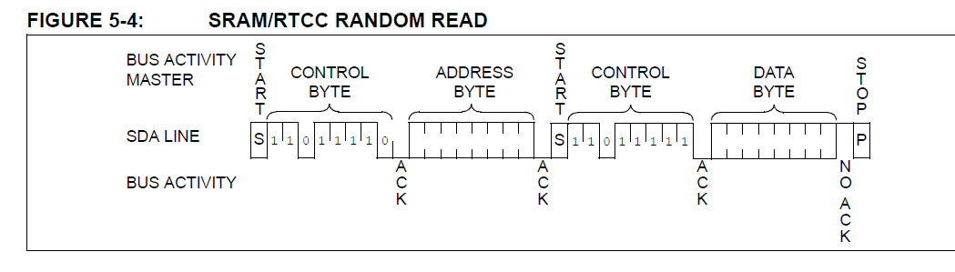
The rtc 7 bit slave address is 0xDE. And they have registers which needs to be accessed according to their datasheet. As per your library for TWI I only see a function such as nrf_drv_twi_tx(nrf_drv_twi_t const * const p_instance, uint8_t address,uint8_t const * p_data,uint32_t length, bool xfer_pending); which doesn't have registers.

If you could please help me how to Read/Write data into the I2C and to its Registers.

Regards Darshan N

  • The nrf_drv_twi_tx() function doesn't have registers because registers isn't anything to do with the actual I2C protocol. I2C is just a data read/data write protocol which does exactly that, writes a chunk of data to a device at an address and reads data back from a device at an address.

    The chip you're interfacing with may be explained in the datasheet using registers, but if you read it again you should see the underlying basic I2C data transfer which accesses them is just a data transfer with a given format. Often for instance, the 'register' number you're writing to is the first byte of the data transferred, and the rest of the data is what's then written to that 'register'. A transfer may consist of writing a byte with a register number in the written data, and then reading, the chip then sends the contents of that 'register' out.

    Once you've understood the basic command sequence to your RTC chip and know how to format the data, then you'll see the function above is exactly what you need, it just sends out a chunk of formatted data.

  • Thank you ,

    Can you please explain me with a few steps for write operations using nrf_drv_twi_tx(); functions? I have attached the screenshot of byte write sequence as per the datasheet .

    SRAM in I2C register starts from 0x20; and SLAVE/DEVICE ADDRESS is 1101111 or 0x6F.

    byte write.PNG

    control byte is READ/WRITE.

    ADDRESS BYTE is slave register.

    I2c code.txt

    READ CYCLE

    byte read.PNG

    RTC DATASHEET

    rtc chip smart switch.pdf

  • I don't use it but .. it must be something like this

    Your slave address is 0xDE, you said, that's the pre-shifted one, Nordic uses just the 7 bits, so it's 0xDE >> 1 or 0x6F. That diagram shows a standard I2C transaction (you should read the spec) so the first byte is the address, shifted, finishing with a '0' which means 'write'.

    So assuming you want to write 0x12 to the register with address 0x20 and you've set the TWI up already

    static uint8_t data[2]; // should be a static buffer especially if you're using the callback mode
    data[0] = 0x20;
    data[1] = 0x12
    nrf_drv_twi_tx( &instance, 0x6F, data, 2, xfer_pending );
    

    instance is the instance you set up, xfer_pending depends on what you're doing (ie are you going to do a repeated start to read data back). That writes out the address and two bytes of data to TWI.

  • Thank you

    I followed your procedure and did the same for read. And I am not able to read in debug mode.

    ALL the pins are connected properly double checked the PCB with my schematics. And the slave is responding have an LED for response which glows.

    please find my code and read cycle attached in my previous answer above.

    can you help me for READ CYCLE ??

Related