When designing a PCB with nRF51, nRF51822 or nRF51422, there are some rules that should be followed in order to get a good working radio/system, with a maximized range.
General rule
The RF part of the schematic and layout should be a copy of our reference design. It means that not only the component values, but also the geometry, relative placement of the components with respect to each other, and the lengths of the transmission lines should be the same as in our reference design. The reference design for both nRF51822 QFN and WLCSP package can be donwloaded from the nRF51822 webpage --> "downloads" --> "reference layout".
Matching networks
In RF, things work differently than in "regular" electronics, due to high frequencies (and short wavelengths). One of the resulting effects is that the phase of a signal will vary along the transmissions lines, as opposed to low frequencies where the wavelengths >> transmission lines, and this effect can be disregarded. If the system (chip and antenna) is not matched, there will be reflections of the signal in the transmission line, resulting in loss. The system can be matched using a 50 Ohm reference point; matching the chip and the antenna to 50 Ohm.
Matching the chip to 50: There are two ways to match the chip to 50 Ohm, using a discrete matching network (QFN only), or using a balun. The performance of the discrete matching network and a balun, is the same. In general, what makes the choice between the two, is the space left on the PCB, since a balun requires less space.
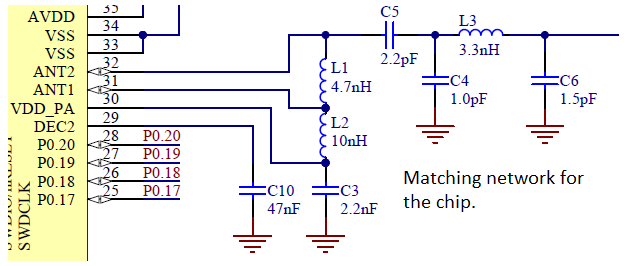
Discrete matching network: the discrete matching network that should be used is provided in the reference design, and it consists of all the components connected from the pins ANT1 and ANT 2. It is very important that this matching network is copy of the reference design, as explained in "general rule". The whitepaper "Tuning the nRF24xx matching network" explains the how this matching network can be tuned, if needed. The whitepaper is written for the nRF24LE1, however, the principle is the same for the nRF51.
Balun: Only baluns that are designed for the specific nRF51 packages, QFN or WLCSP, should be used. Since the impedance on ANT1 and ANT2 is different on the WLCSP and QFN packages, their baluns cannot be interchanged. The list of baluns that can be used can be found on the nRF51822 webpage --> "development tools and software". The placement of the baluns should be an exact copy of the reference layout in their datasheet.
The baluns the can be used with the nRF51 are the following:
-
QFN: 2450BM14E0003 from Johanson Technology
-
WLCSP: 2450BM08B0003 from Johanson Technology
-
WLCSP: BAL-NRF02D3 from ST
-
WLCSP: TBL-1411-245-LR from Cyntec
-
WLCSP: LFB182G45BG7x948 from Murata
In addition to matching the chip to 50 Ohm, the above solutions will also damp harmonics and RX LO, which is required for the design to pass the various regulatory standards. The whitepaper "Regulatory and Compliance Standards for RF Device" sums up the most common regulatory standards.

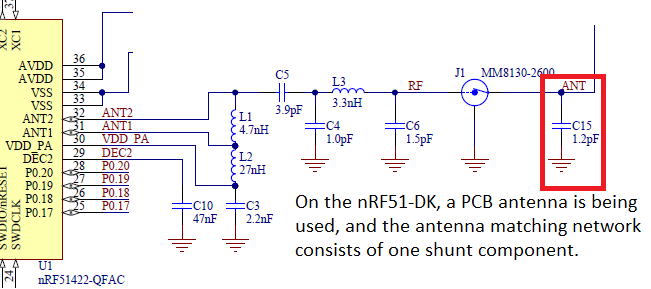
Matching the antenna to 50 Ohm: There are basically two types of antenna matching networks; pi-network and a matching network consisting of one shunt component only. The type of antenna decides which matching network to use. If using a PCB antenna, the matching network should consist of one shunt component, and if using a chip antenna, the matching network should be a pi-network. The value(s) of the component(s) in the matching network will have to be found during tuning, by doing measurements using a network analyzer. The reason for this is that the impedance of the antenna depends on its close environment; it means that the measurements on a device should be performed when the device is placed in its final housing, in a similar environment to where it is supposed to be used. It is not possible to calculate the value(s) for the component(s) in the matching network, because there are too many parameters to take into account. The "Antenna tuning" whitepaper explains more about why tune the antenna, and how to do it.

In a design, the antenna matching network should be placed in between the matching network for the chip and the antenna.
Antenna
There are two types of antennas that can be used, a PCB antenna or a chip antenna. Under optimal conditions, the performance of a PCB antenna and a chip antenna will be more or less the same.
PCB antenna: The whitepaper "Quarterwave printed monopole antenna for 2.4GHz" explains how to design a PCB antenna.
Chip antenna: Any 2.4 GHz antenna can be used. In order to obtain good performance, it is important to place the antenna according to its datasheet. The antenna datasheet will also contain information about the bandwidth of the antenna.
Ground planes
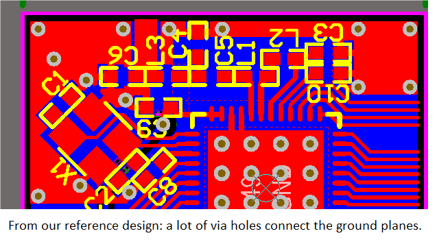
A typical design consists of two ground planes; a top ground plane and a bottom ground plane. Both ground planes should preferably be as large and solid as possible. Ground is the reference of the system, the impedance of the antenna should for example be 50 Ohm with respect to ground. The larger the ground planes are, the more it takes to disturb them. The two ground planes should be connected using a lot of via holes. Our reference designs show what the distribution of the via holes may look like.

Crystal and load capacitors
Crystal: On the nRF51, an external 16 MHz crystal is mandatory, and an external 32 kHz crystal is optional. When choosing a crystal, it is important that it is with the specifications given in the nRF51822/nRF51422 Product Specification, chapter 8.1 ("Electrical specifications --> Clock sources").
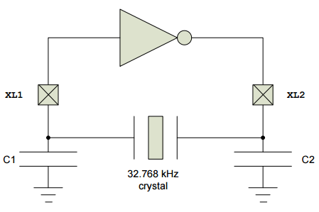
Load capacitors: The load capacitors are the capacitors connected to the crystal, C1 and C2 connected to the 16 MHz crystal in our reference design, and C13 and C14 for the 32 kHz crystal.The value of these capacitors can be found using the following formula:
C1 = C2 = 2Cl - C_pcb - C_pin
Cl: Load capacitance of the crystal (found in the crystal datasheet)
C_pcb + C_pin is approximately 4 pF.

The whitepaper "Crystal Oscillator Design Considerations" explains more about the topic.
Measuring the frequency of the 16 MHz crystal should be done by measuring the carrier frequency of the radio. If the carrier frequency of the radio is within the specifications, the 16 MHz crystal is also within the specifications. If trying to probe the crystal directly, the frequency of the crystal will drift, because the probe possesses a capacitance, and this will effectively change the total value(s) of the load capacitors.

