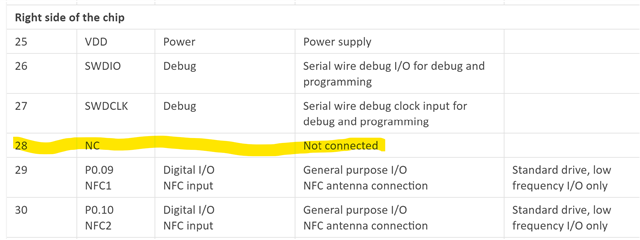
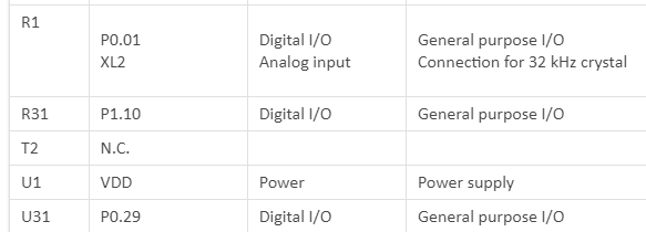
Pins marked as n.c. in datasheet nRF5340-QKAA. What to do with them on the PCB?

The datasheet list 

A25, B12, B26, D2, F2, G1, H2, J31, K2, T2, AG31, as N.C.

I have not been able to read exactly what N.C. implies: It could be: "do not connect", "no internal connection".

If one for clarification looks at the example circuits in the dataheet some of these pin, but not all are connected to Vss (gnd)

The connected pins are:

A25, B12, B26,              G1, H2, J31 

So it means that D2, F2, K2, T2, AG31 are left unconnected. A bit unclear which rule to follow.

Bottom line of my question: what is the required connection for pins marked N.C.

Thanks

Parents Reply
  • but please when updating you documentation: Think in the terms of the user and do not just mark not connected. The user need to know what that implies with respect to the use of the part.

    I.e. It can mean:

    1. Do not connect any copper but the solder pad to this pin
    2. No internal connection - You can connect to this pad if you need to pass through with a trace

    So N.C. need to be specified. For nRF5340 I deduce that it is option 2 which applies.

    And now I will stop.

Children
Related