I'm working with a nRF52840 DK connected with SCL, SDA, GND, VDD to my custom PCB. I'm using the nRF5_SDK_17.1.0.ddde560.
My apologies in advance if I missed anything obvious, as I am new to development with nRF.
I'm trying to communicate with the ADS1114 through a TCA9517A bus level shifter, as the ADS1114 has a supply voltage of 5V. The I2C communication often works, and seems to keep working, but sometimes the bus seems to get stuck. The project is based on the pca10056 twi_sensor example project, I mainly changed the registers to write.
I've looked at the other posts related to TWI problems, but I did not find a solution to this issue there, unfortunately.
I am using external pullups (~3k) and have disabled the internal pull-ups.
I analysed the I2C bus with a logic analyser and oscilloscope, but I feel like I lack the experience to figure out what exactly is going on, so I would really appreciate any insights into the problem or what steps I could try to fix it.
Failed communication example
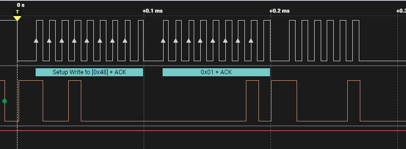
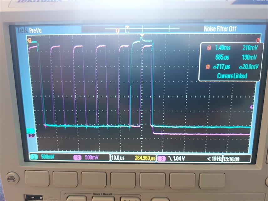
With the scope images of the final CLKs before communication fails (blue is SDA, purple is SCL):
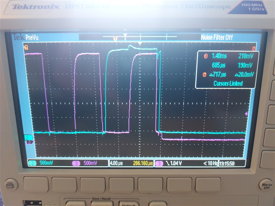
Succesfull transaction example

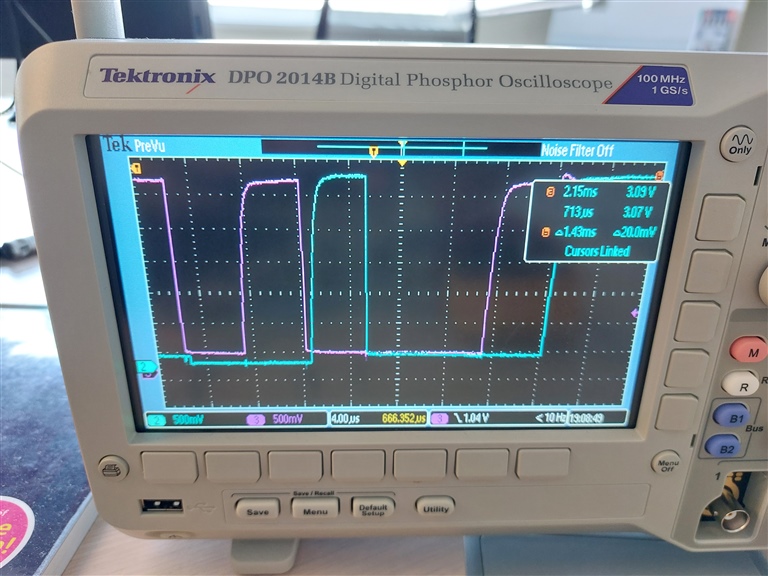
The error doesn't always occur at this spot, but the cases look like this.
When this error occurs, the code gets stuck at the 'while (m_xfer_done == false);' that is after the transaction.
To me the biggest difference seems to be the pull down of the SCL signal to a voltage level lower than the other pull-down levels. There's also what appears to be a small 'glitch' in the SDA before this happens, but I am not sure if this is related. I looked at the ADS1114 datasheet, and it says the device does not implement clock stretching nor does it drive the SCL pin. It is almost as if the master just stops driving the CLK.
I get the impression that if the initial transfer (configuration write, address pointer write, first few reads) is succesfull, it continues to work indefinitely. Therefore I might be able to just keep on retrying until it is succesfull by implementing a recovery system. Do you have any pointers to how I would succesfully implement this?
Source code
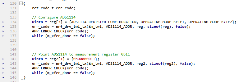
For some more context, here is the code of the main transactions (note, LM75B_ADDR is the ADS1114 address):
/* Mode for ADS1114. */#define OPERATING_MODE_BYTE1 0b10000100 //0x84#define OPERATING_MODE_BYTE2 0b10000011 //0x83
void ADS1114_CONFIG(void){ ret_code_t err_code;
/* Writing to LM75B_REG_CONF "0" set temperature sensor in NORMAL mode. */ uint8_t reg[3] = {LM75B_REG_CONF, OPERATING_MODE_BYTE1, OPERATING_MODE_BYTE2}; err_code = nrf_drv_twi_tx(&m_twi, LM75B_ADDR, reg, sizeof(reg), false); APP_ERROR_CHECK(err_code); while (m_xfer_done == false);
/* Writing to LM75B_REG_CONF "0" set temperature sensor in NORMAL mode. */ uint8_t reg2[1] = {0b00000011}; err_code = nrf_drv_twi_tx(&m_twi, LM75B_ADDR, reg2, sizeof(reg2), false); APP_ERROR_CHECK(err_code); while (m_xfer_done == false);}
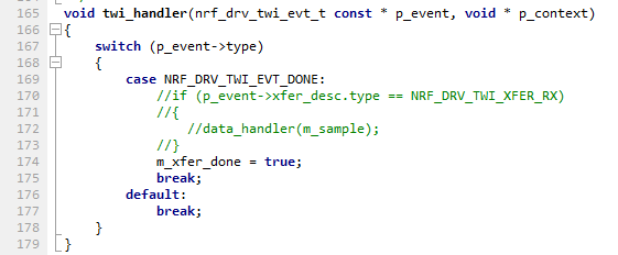
void twi_handler(nrf_drv_twi_evt_t const * p_event, void * p_context){ switch (p_event->type) { case NRF_DRV_TWI_EVT_DONE: //if (p_event->xfer_desc.type == NRF_DRV_TWI_XFER_RX) //{ //data_handler(m_sample); //} m_xfer_done = true; break; default: break; }}
void twi_init (void){ ret_code_t err_code;
const nrf_drv_twi_config_t twi_lm75b_config = { .scl = ARDUINO_SCL_PIN, .sda = ARDUINO_SDA_PIN, .frequency = NRF_DRV_TWI_FREQ_100K, .interrupt_priority = APP_IRQ_PRIORITY_HIGH, .clear_bus_init = true };
err_code = nrf_drv_twi_init(&m_twi, &twi_lm75b_config, twi_handler, NULL); APP_ERROR_CHECK(err_code);
nrf_drv_twi_enable(&m_twi);}
static void read_sensor_data(){ m_xfer_done = false;
/* Read 1 byte from the specified address - skip 3 bits dedicated for fractional part of temperature. */ //ret_code_t err_code = nrf_drv_twi_rx(&m_twi, LM75B_ADDR, &m_sample, sizeof(m_sample)); ret_code_t err_code = nrf_drv_twi_rx(&m_twi, LM75B_ADDR, samples, sizeof(samples)/sizeof(samples[0]));
APP_ERROR_CHECK(err_code);}
Sidenotes
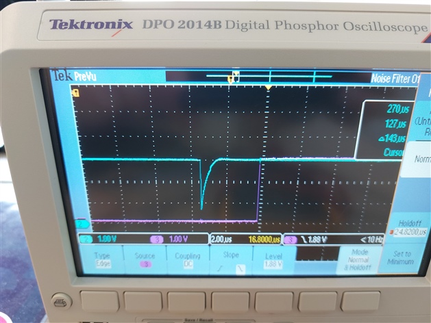
- Occasionally, the first write fails entirely and this could be seen on the scope, although I am not 100% sure if this is related to the issue (here, purple was a custom output pin set high at start):
- Sometimes if I keep the development kit running for a bit, I get a random J-link error. This might be because it is stuck waiting for the transaction to finish.
Some more context:
- I am using SEGGER Embedded Studio for ARM V7.30 on Windows 10
Any advice and help is appreciated. If more information is required, please let me know.
Kind regards,
Frederik


