
Hi there, we have a product that we initially prototyped with a SARA-R4 modem, but are pivoting to the nrf9160 platform because of the extreme power saving and simplicity of Zephyr development. I am in the process of redesigning our board, with the nrf9160 at the core, and am unable to find documentation or recommended design examples for a programming header on our custom board. If anyone has any insight or can point me towards better documentation, it would be very much appreciated.
Specifics:
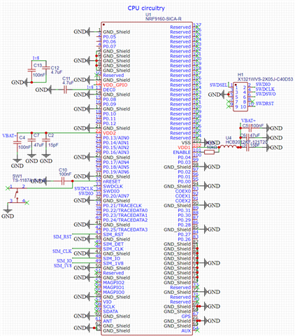
- According to https://infocenter.nordicsemi.com/index.jsp?topic=%2Fug_nrf91_dk%2FUG%2Fnrf91_DK%2Fhw_debug_out.html, P19 on the nrf9160-DK can act as a programmer to flash firmware to our custom PCB.
- I cannot find documentation on SWD0_SELECT, SWD0_RESET, or SWD0_SWO connections for a standalone/embedded nrf9160. Are they required to program the custom board or do we only need SWD0_CLK<->SWDCLK and SWD0_IO<->SWDIO and GND<->GND connected between the nrf9160-DK and our custom nrf9160 board?
- A photo of the nRF9160 section of our current schematic is included with the header design copied from P19 of the DK.
Thank you for your insight.
