About nRF52840 RF filter when using chip antenna

Hi,

I have a question about the antenna circuit.

I'm designing a circuit using nRF52840QFAA and 2450AT14A0100001T(chip antenna). (link of chip antenna ic)

I have two question.

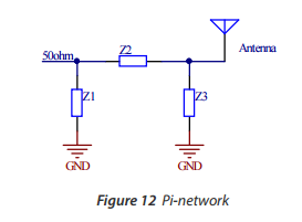
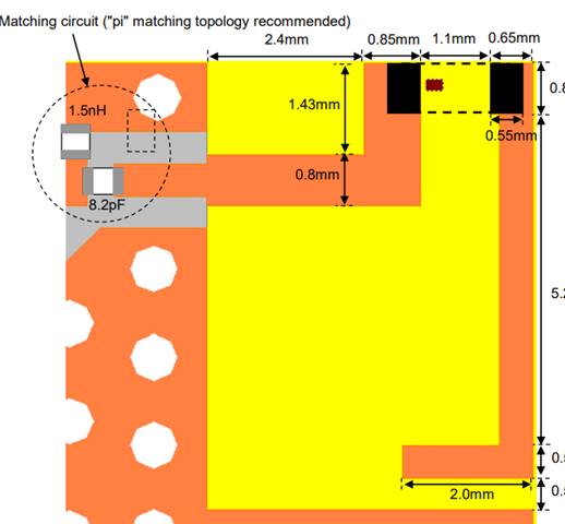
1. In chip antenna datasheet, the matching circuit is 1.5nH and 8.2pF.

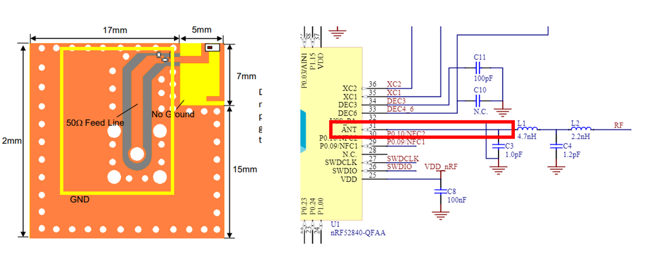
And, in reference circuit in nRF52840QFAA, the inductor and capacitor is 4.7nH, 2.2nH, 1.0pF, 1.2pF.

 Which matching circuit should I refer to? 위치 매칭

2. about 50 ohm feed

Should I design the 50 ohm feed line of nRF52840 as 50 ohm between pin 31 and L1?

Thank you.

Regards,

Youngun

Parents
  • Hello,

    You need to copy the layout and schematic exactly for the ANT circuitry shown for the package variant you choose, the reference schematic and layout is found here:
    https://www.nordicsemi.com/Products/nRF52840/Compatible-downloads?lang=en#infotabs 

    So this means that you need to copy exactly (including layout) for L1, L2, C3 and C4 in the the screenshot you show.

    After L2 you can place the matching components and layout recommended by the antenna manufacturer, I can see in your screenshot that they recommend a PI matching topology. Example of PI network is found here. This PI network must be placed between L2 and the chip antenna: 

    The final component values in the PI network must be found by measurement on the final PCB, but as a starting point you can use the values listed in the datasheet (1.5nH and 8.2pF I think you write, the last component be left not placed for now).

    Kenneth

Reply
  • Hello,

    You need to copy the layout and schematic exactly for the ANT circuitry shown for the package variant you choose, the reference schematic and layout is found here:
    https://www.nordicsemi.com/Products/nRF52840/Compatible-downloads?lang=en#infotabs 

    So this means that you need to copy exactly (including layout) for L1, L2, C3 and C4 in the the screenshot you show.

    After L2 you can place the matching components and layout recommended by the antenna manufacturer, I can see in your screenshot that they recommend a PI matching topology. Example of PI network is found here. This PI network must be placed between L2 and the chip antenna: 

    The final component values in the PI network must be found by measurement on the final PCB, but as a starting point you can use the values listed in the datasheet (1.5nH and 8.2pF I think you write, the last component be left not placed for now).

    Kenneth

Children
No Data
Related