How to program an external board using a DK board?

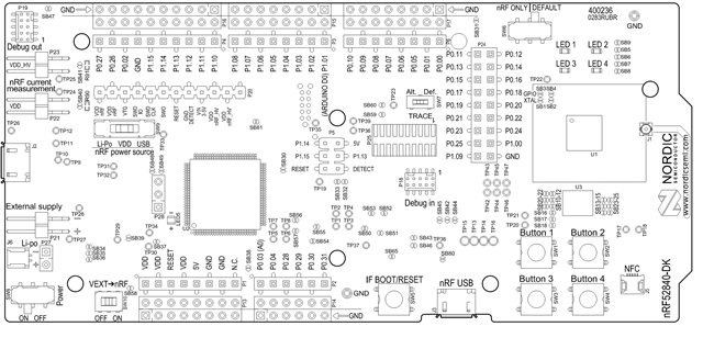
Before I start, I beg that any responses do NOT link to any other threads. There are 20 threads across the internet in different forums documenting how they got external programming to work, but the biggest issue is that they're all different, and use different boards. For example, my version of the nRF52840 DK doesn't even have the 'GND DETECT' pin that's listed in the very documentation for the board.

This area is massively lacking, and following the official documentation, I've bricked two external boards... not impressed.

I have two boards, an itsy bitsy nRF52840 Express and an nRF52840 DK. I'm using Zephyr Project RTOS, but I'm using 'Programmer' in 'nRF Connect for Desktop' to actually upload through the DK board to the itsy bitsy.

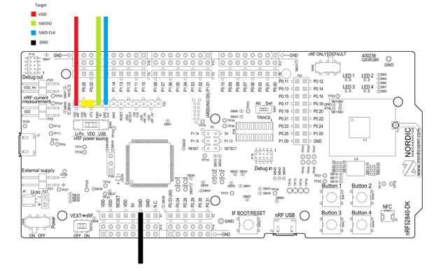
My connections are as follows:

DK              |         Itsy Bitsy

GND          -->      GND

VDD nRF   -->      VDD

SWDIO      -->      SWDIO

SCLK         -->      SCLK

The programmer says it's complete, but the itsy bitsy doesn't seem to be doing what I programmed it to do (output HIGH on pin 10).

The concerning part is that holding the RST or SW pins on the itsy bitsy no longer trigger the bootloader mode (though this could be because I erased any bootloaders in uploading using the DK board).

I'm totally lost, developing with nRF chips just feels like chasing one senseless issue after another.

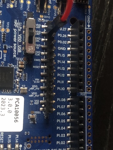
The nRF52840 DK pinout below, which is in the official documentation does NOT match the pinout I see on my board, which I will post below the other image.

Parents
  • Solved! For anyone with a similar issue, here's what I found and how I solved it.

    1. The official documentation severely lacks in some areas, and this is one of the worst areas. The official documentation ambiguously suggest methods that can fry not only the target board but also your really expensive and important development board. Actually, in the same section for other chips (such as nRF52832), it makes it very clear what not to do, however, the nRF52840 does not get this warning, despite the same risk being present (ask me how I know...).

    2. The documentation is not just ambiguous, it's downright incorrect, as is the silkscreen on my board. Despite the difference in pin names on my silkscreen, I decided to try external programming using not the same pin names as other forum posters' diagrams, but actually the same physical pin locations, despite a discrepancy in apparent silkscreen pin names. This is the THIRD (and none of them related) silkscreen pin labeling error I've seen on this (nRF52840) dev board.

    Here's the pin layout that worked for me:

    Make sure to bridge the two pins with yellow covering them in that image.

    ONLY plug in the programming board, DO NOT plug in the target/external board. The target/external board should ONLY be getting power from the connections to the programming board.

    As for extrapolating this information to another DK board (like nRF52832 DK or nRF52833 DK), this part is not as clear to me since what works for me is NOT what the official documentation describes... however, the basics should be similar.

    Programmer SWDIO to Target SWDIO

    Programmer SWD CLK to Target SWD CLK

    Programmer VDD nRF to Target VDD

    Programmer GND to Target GND

    Programmer set to external programming (as opposed to internal). For the nRF52840 DK, this is achieved by bridging the two pins covered in yellow in my colored diagram. These two pins are VTG and VDD nRF'.

Reply
  • Solved! For anyone with a similar issue, here's what I found and how I solved it.

    1. The official documentation severely lacks in some areas, and this is one of the worst areas. The official documentation ambiguously suggest methods that can fry not only the target board but also your really expensive and important development board. Actually, in the same section for other chips (such as nRF52832), it makes it very clear what not to do, however, the nRF52840 does not get this warning, despite the same risk being present (ask me how I know...).

    2. The documentation is not just ambiguous, it's downright incorrect, as is the silkscreen on my board. Despite the difference in pin names on my silkscreen, I decided to try external programming using not the same pin names as other forum posters' diagrams, but actually the same physical pin locations, despite a discrepancy in apparent silkscreen pin names. This is the THIRD (and none of them related) silkscreen pin labeling error I've seen on this (nRF52840) dev board.

    Here's the pin layout that worked for me:

    Make sure to bridge the two pins with yellow covering them in that image.

    ONLY plug in the programming board, DO NOT plug in the target/external board. The target/external board should ONLY be getting power from the connections to the programming board.

    As for extrapolating this information to another DK board (like nRF52832 DK or nRF52833 DK), this part is not as clear to me since what works for me is NOT what the official documentation describes... however, the basics should be similar.

    Programmer SWDIO to Target SWDIO

    Programmer SWD CLK to Target SWD CLK

    Programmer VDD nRF to Target VDD

    Programmer GND to Target GND

    Programmer set to external programming (as opposed to internal). For the nRF52840 DK, this is achieved by bridging the two pins covered in yellow in my colored diagram. These two pins are VTG and VDD nRF'.

Children
No Data
Related