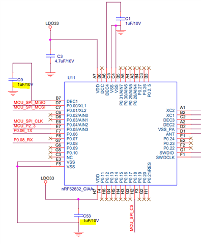
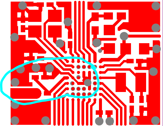
Dear Nordic Engineers
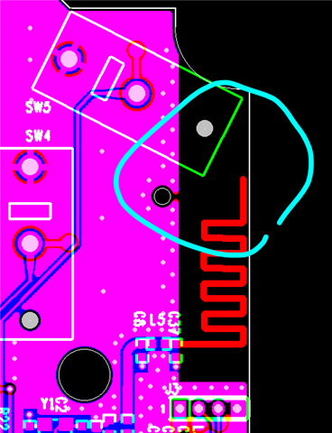
The following files is our customer's hardware design. Please help me review them, and if it has some unreasonable design, please give me some good suggestions.
Best regards.
Hannibal
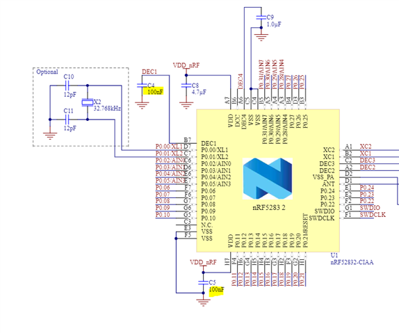
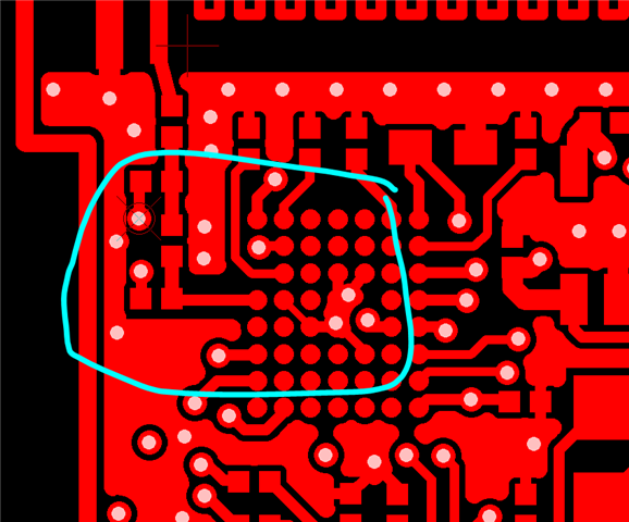
Dear Nordic Engineers
The following files is our customer's hardware design. Please help me review them, and if it has some unreasonable design, please give me some good suggestions.
Best regards.
Hannibal