Hello,
I am currently using the HJ-840 SiP module that employs the nRF52840 SoC with an onboard chip antenna, 2450AT18B100E (Johanson Technology).
I am now facing some layout design issues. I'm still a beginner in this area; please excuse any shortcomings.
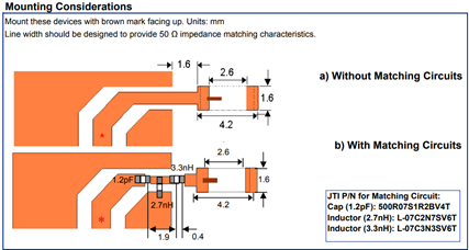
Since I have previously contacted their FAE, they advised me to use an external ceramic antenna, preferably connected through a PI.
Below is my SCH design diagram.
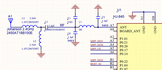
The capacitor and inductor are chosen and configured based on the specifications provided in the datasheet.
I now want to start drafting the layout design, but there are still details I'm uncertain about.
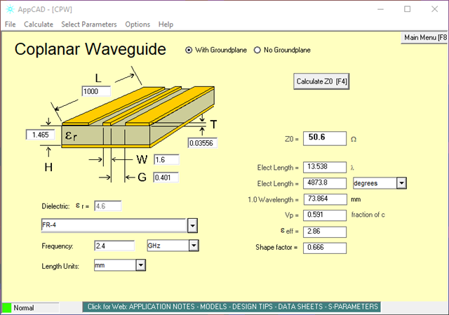
I used AppCAD and the impedance matching calculator from JiaLiChuang (JLC) Company to compute the trace width.
The following are the results I derived, as shown in the diagram.
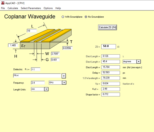
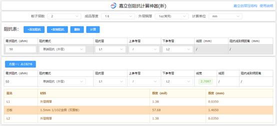
(The green number 2.7097mm represent the trace width, and the orange number 1.465mm indicates thickness.)
I'm likely going to use a double-layer board and design using single-ended impedance, with a copper thickness of 1oz.
However, I'm still uncertain why the computed trace width is so wide. Is this normal?
(Compared to the lines drawn on the datasheet for connecting capacitors and inductors, it's much thicker.)
How should I proceed with such a design? Are there other considerations I should be aware of during the layout?
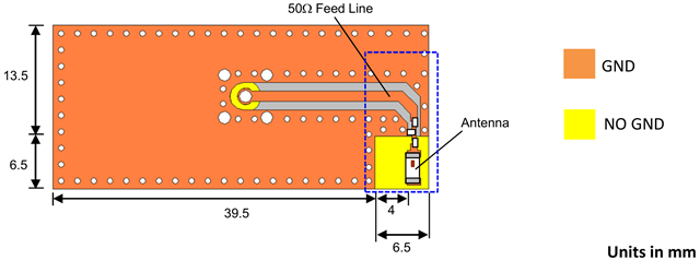
(For instance, the antenna should be placed at the edge of the board, the surrounding area should be kept clear, and copper should not be spread, etc.)
Thank you for reading.