
Hello,
I am new to RF/antenna matching stuff. I have an nRF24LE1 product and I simply cannot understand how to get the component values which are shown in the Altium files and guides. For reference here is the circuit for nRF24LE1F16Q24, the datasheet gives the ANT1/ANT2 impedance as 15+j88. From that, I would assume that we want the rest of the circuit connected to that to look like 15-j88. If its as simple as that theoretically, can someone who understands this provide a worked example of how these component values were arrived at? Maybe post an output from Smith.
Also noting the series LC circuit gives an equivalent +j44 @2.4GHz so why not use an inductor of half its value instead of the two components? Practical value reasons?
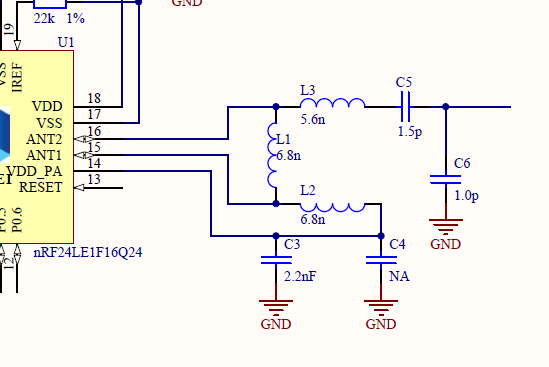
The line connected to C6/C5 which goes nowhere, does that indicate an antenna? If a chip antenna is involved, does that change everything?
Oh, one more question, what does ANT1/ANT1 look like electrically? A balanced source with 7.5 + j44 per side?
If I was to model this, say with Smith, does it need 50 Ohms sections between each component to simulate the PCB traces?
Much gratitude to anyone who can educate me.
