Hi,
I have been designed a couple of PCBs using STM32 MCUs and got them manufactured & assembled through JLCPCB and this is my first project designing a PCB using nRF SoC. I have several queries, to be honest, regarding my nRF 52840 based PCB before placing manufacturing/ assembling order at JLCPCB. I will try to give you as much detail as possible and I am following nRF52840 Reference Design Config-2.
1. Power Supply
As far as I know, there are three ways to supply power to nRF52840: VBUS (5V from USB), VDDH (roughly 2 to 5.5V) and VDD (3V3). I am using 3.7V Li-Po battery to power this SoC and, as such, connected +ve of battery to VDDH only. The screenshot of my schematic is:
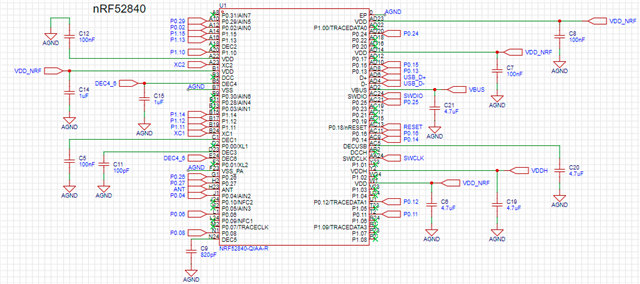
- Do I need to connect any other power supply (besides not required by me)?
- I have not used VBUS, so I can remove C21 (4.7uF)?
- If, I connect power to VDDH, do I get regulated VDD from SoC?
- In Reference Design, what is meant by Vext? It is for supplying load to external components or otherwise?
2. Not Connected Components
Reference Design has several NC components and, besides, I also have several pins not connected as shown in the above screenshot.
- Do I need NC in my design such as C10, C13, C22?
- I do not need RTC function and, as such, not used optional 32.768KHz external oscillator. I left pins unconnected, I hope this is fine. I am using following, 32MHz crystal OSC.
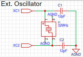
- C9 is required for this design, I have included it to be on safe side.
- I have not used NFC, USB, DCC and DCCH pins and left them unconnected.
- Regarding Reset pin, can I leave it unconnected?
- Do I need Tracedata pins for debugging?
3. Battery Charging Circuit
I have used following circuit for battery charger indicator.
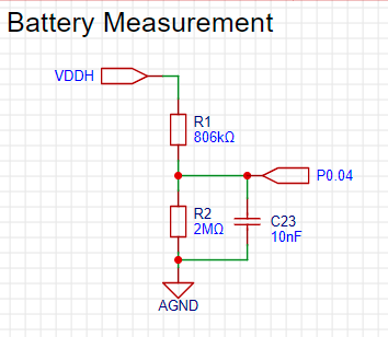
- This is fine?
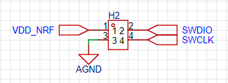
4. Programming through SWDIO/ SWDCLK
I will not be using USB in my first design due to space limitation and will be using SWD for this purpose. I have STLink & nRF52840 DK, can I use STLink to program (bootload/ flash) this nRF52840 by supplying VDD(3V3), Gnd, SWDIO & SWCLK?
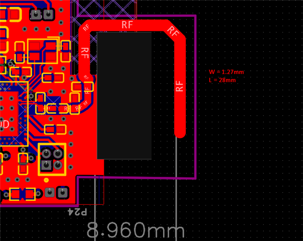
5. Antenna
This is major area of my concern, besides, I have specific PCB dimension requirement i.e. 24x30mm. For Antenna, I have followed nRF52840 monopole anternna design and used the same components as of nRF52840 DK. Antenna's schematic and PCB are as follow:
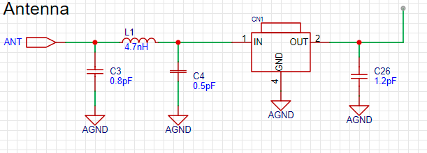
- Due to space/ width limitation, I have placed SMA connector at top by extending trace from C4 to SMA, this will require matching at end? If, so, what is the easiest procedure?
- Also, as per antenna design paper, I need to keep at least 10mm distance between antenna and ground plane, this has also increased width of PCB beyond 6mm of the requirement. Which antenna would you suggest for limited space? Any reference design giving matching components and antenna design.
- Can I connect small, wire type, antenna to SMA connector without this PCB antenna? Please provide any such antenna type.
- Please list any other compact and reasonable chip antenna considering space limitation.
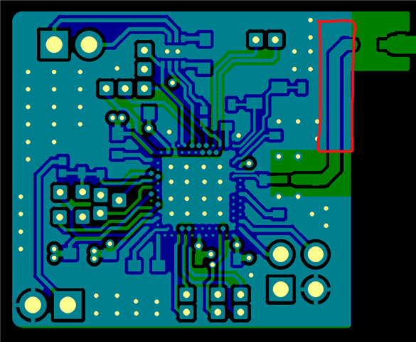
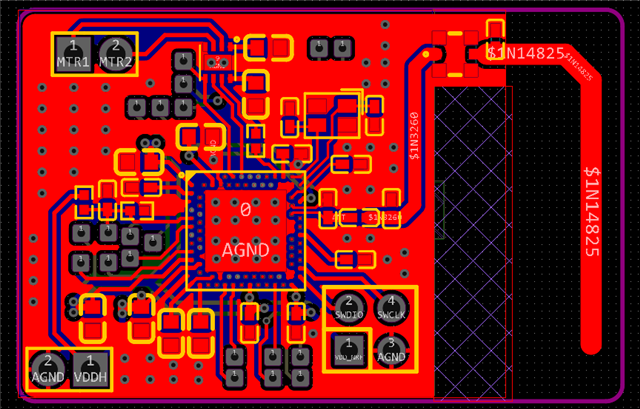
6. PCB Layout & Routing
I have followed nRF52840 Reference Design but I need to make sure everything is reasonably correct before placing order. I have attached my gerber files.
- Please see the layout if it seems reasonable without any obvious/ significant flaw. There were few DRC errors of clearances at 0.15mm as opposed to rule having 0.152mm which I changed to 0.152mm.
I know, I have a long list of queries and would be grateful for this support.
Thanks
Shahid