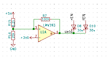
Level based control of GPIOTE


Hi,

I have a comparator acting as a UVLO, it connects to a NRF52 pin with a pull-up. The comparator also pulls down two other circuits using a diode, which in turn are connected to other NRF52 pins using pull-ups. It works well.

I'd like if possible to remove the diodes and connecting the UVLO signal via GPIO Event through PPI and controlling the other two pins via GPIOTE SET and CLEAR.

What I can't determine from the datasheet is whether once the initial output of GPIOTE is set if PPI & GPIOTE are fully async to the clock in which case it would be like level control where they couldn't miss an event, or whether the clock is working to determine the event (like a D gate) in which case potentially the event could be missed.

It is only a small optimisation but one I thought I'd look at as I was contemplating moving the comparator to the built-in one.

Andrew

Parents
  • Hi,


    What I can't determine from the datasheet is whether once the initial output of GPIOTE is set if PPI & GPIOTE are fully async to the clock in which case it would be like level control where they couldn't miss an event, or whether the clock is working to determine the event (like a D gate) in which case potentially the event could be missed.

    If I understand the scenario correct, you want two IN channels to, based on falling/rising edge-triggering, SET/CLR two other GPIOs. Please correct me if I'm mistaken.

    GPIOTE IN/OUT, when connected through PPI, will be synchronous to the internal 16 MHz peripheral clock.

    If more than one operation occurs on the same clock cycle, one event can be postponed to the next clock cycle.


    There is however one scenario that can occur, which is errata #155:

    https://infocenter.nordicsemi.com/topic/errata_nRF52810_Rev3/ERR/nRF52810/Rev3/latest/anomaly_810_155.html?cp=5_5_1_0_1_12


    If you have two GPIOTE IN channels occurring within the timed scope (ie. < 1.3 us apart), you will hit this errata. 

    The side-effect of this errata workaround is higher current consumption, as the peripheral clock tree will be kept in sleep mode.


    Kind regards,

    Håkon

  • Hi,

    LMV393 has a propagation of 0.2us, which is 5 MHz.

    As you say it's synchronous to the 16MHz clock, so let's say at max there are 5 edges at 0.2us apart. Would PPI/GPIOTE be able to keep up driving an output pin using the SET/CLEAR events?

    It sounds like it would, so long as the propagation didn't take more than 3 clock cycles.

  • Hi,

    Sorry that's an error (now corrected), the PPI event controls two pins, front and rear (I haven't tested this revised code yet, awaiting pcb arrival this week). The event actually controls three pins, but PPI only supports the single fork so I use two channels. Also one of the channels doesn't use the SET event.

    No, I am now using NRF_COMP. I managed to make a pin available, but whether it's comparator or gpiote input the query remains the same. :)

    All that matters is:

    a) ensure the comparator is level high
    b) set the gpiote pin high
    c) do the above atomically - the comparator can't go low between a and b.

    I occasionally need to override the GPIOTE output. At that point when I turn it back on it is not necessarily in sync with the comparator output. This is the problem with events rather than levels. Anyhow, it is a condition I must resolve.

    Simplied init:

      // gpiote
      NRF_GPIOTE->CONFIG[CFG_GPIOTE_POWERMANAGER_FRONT] = GPIOTE_CONFIG_MODE_Disabled << GPIOTE_CONFIG_MODE_Pos | CFG_PIN_POWERMANAGER_FRONT_ENABLE << GPIOTE_CONFIG_PSEL_Pos;
      
      // ppi
      NRF_PPI->CH[CFG_PPI_POWERMANAGER_UVLO_FRONTREAR_GOOD].EEP = (uint32_t) &NRF_COMP->EVENTS_UP;
      NRF_PPI->CH[CFG_PPI_POWERMANAGER_UVLO_FRONTREAR_GOOD].TEP = (uint32_t) &NRF_GPIOTE->TASKS_SET[CFG_GPIOTE_POWERMANAGER_FRONT];
      NRF_PPI->CH[CFG_PPI_POWERMANAGER_UVLO_FRONTREAR_BAD].EEP = (uint32_t) &NRF_COMP->EVENTS_DOWN;
      NRF_PPI->CH[CFG_PPI_POWERMANAGER_UVLO_FRONTREAR_BAD].TEP = (uint32_t) &NRF_GPIOTE->TASKS_CLR[CFG_GPIOTE_POWERMANAGER_FRONT];
     
      NRF_PPI->CHENSET = 1 << CFG_PPI_POWERMANAGER_UVLO_FRONTREAR_GOOD
        | 1 << CFG_PPI_POWERMANAGER_UVLO_FRONTREAR_BAD;
    
      // UVLO
      NRF_COMP->REFSEL = UVLO_REFERENCE << COMP_REFSEL_REFSEL_Pos;
      NRF_COMP->TH = UVLO_HYSTERESIS_UP << COMP_TH_THUP_Pos | UVLO_HYSTERESIS_DOWN << COMP_TH_THDOWN_Pos;
      NRF_COMP->PSEL = COMP_UVLO << COMP_PSEL_PSEL_Pos;
      NRF_COMP->ENABLE = COMP_ENABLE_ENABLE_Enabled << COMP_ENABLE_ENABLE_Pos;
    

    Imagine you want to override GPIOTE output, by toggling GPIOTE_CONFIG_MODE_[Disabled|Task], and when you choose task it must give the same output as the current comparator state.

    Perhaps calling COMP.SAMPLE will fire and propagate the correct event?...

    Andrew

  • I may have a solution, if I leave GPIOTE Task enabled but instead switch GPIO to be an input with a pull-down enabled...?

    edit: datasheet suggests not. infocenter.nordicsemi.com/index.jsp

  • I think I have it. The UVLO is triggered by the two downstream circuits controlled by these enable pins, and the circuits are bucks which turn off fast and turn on slower. With that in mind when I want to turn either on...

    1. turn both off using GPIOTE_CONFIG_MODE_Disabled
    2. the comparator will now be in high.
    3. Turn an output on using GPIOTE_CONFIG_MODE_Task and OUTINIT=high
    4. Turn on the other output if it were already enabled.

    Given the speed/delay of the buck(s) turning on the comparator event wont fire between steps 3 and 4 so all will be in sync.

  • Hi,


    snoopy20 said:
    1. turn both off using GPIOTE_CONFIG_MODE_Disabled

    This will disable GPIOTE channel, and not really do anything with the state of the GPIO itself.

    This is highly likely not the functionality you're after.

    snoopy20 said:
    I may have a solution, if I leave GPIOTE Task enabled but instead switch GPIO to be an input with a pull-down enabled...?

    No, but you can use more PPI channels to ensure that other GPIOTE OUT channels are set in your wanted state at that time.


    Can you share a diagram or similar on how you want your GPIOs to be set in each COMP state?


    Kind regards,

    Håkon

  • This reply was deleted.
Reply Children
  • Been looking into it this evening. I read that GPIO config is retained when GPIOTE takes over the pin output. I'm unsure but making an assumption that weak pull is still operational when pin is in outmode mode. A hopeful solution is:
      

    NRF_GPIO->PIN_CNF[CFG_PIN_POWERMANAGER_FRONT_ENABLE] = pinDisconnectInputBuffer 
        | GPIO_PIN_CNF_DIR_Output << GPIO_PIN_CNF_DIR_Pos 
        | GPIO_PIN_CNF_DRIVE_S0D1 << GPIO_PIN_CNF_DRIVE_Pos 
        | GPIO_PIN_CNF_PULL_Pulldown << GPIO_PIN_CNF_PULL_Pos;
      
    NRF_GPIOTE->CONFIG[CFG_GPIOTE_POWERMANAGER_FRONT] = GPIOTE_CONFIG_OUTINIT_High << GPIOTE_CONFIG_OUTINIT_Pos 
        | GPIOTE_CONFIG_MODE_Task << GPIOTE_CONFIG_MODE_Pos 
        | CFG_PIN_POWERMANAGER_FRONT_ENABLE << GPIOTE_CONFIG_PSEL_Pos;
    
    NRF_PPI->CH[CFG_PPI_POWERMANAGER_UVLO_FRONTREAR_GOOD].EEP = (uint32_t) &NRF_COMP->EVENTS_UP;
    NRF_PPI->CH[CFG_PPI_POWERMANAGER_UVLO_FRONTREAR_GOOD].TEP = (uint32_t) &NRF_GPIOTE->TASKS_SET[CFG_GPIOTE_POWERMANAGER_FRONT];
    NRF_PPI->CH[CFG_PPI_POWERMANAGER_UVLO_FRONTREAR_BAD].EEP = (uint32_t) &NRF_COMP->EVENTS_DOWN;
    NRF_PPI->CH[CFG_PPI_POWERMANAGER_UVLO_FRONTREAR_BAD].TEP = (uint32_t) &NRF_GPIOTE->TASKS_CLR[CFG_GPIOTE_POWERMANAGER_FRONT];
    
    // UVLO
    NRF_COMP->REFSEL = UVLO_REFERENCE << COMP_REFSEL_REFSEL_Pos;
    NRF_COMP->TH = UVLO_HYSTERESIS_UP << COMP_TH_THUP_Pos | UVLO_HYSTERESIS_DOWN << COMP_TH_THDOWN_Pos;
    NRF_COMP->PSEL = COMP_UVLO << COMP_PSEL_PSEL_Pos;
    NRF_COMP->ENABLE = COMP_ENABLE_ENABLE_Enabled << COMP_ENABLE_ENABLE_Pos;
    NRF_COMP->TASKS_SAMPLE = COMP_TASKS_SAMPLE_TASKS_SAMPLE_Trigger << COMP_TASKS_SAMPLE_TASKS_SAMPLE_Pos;
    
    // wait a moment for voltage to stablize
    // if it doesn't happen watchdog will reset
    while (!NRF_COMP->RESULT) {
      NRF_COMP->TASKS_SAMPLE = 1;
    };
    NRF_COMP->EVENTS_DOWN = 0;
    
    // must come after comparator to ensure output sync
    NRF_PPI->CHENSET = 1 << CFG_PPI_POWERMANAGER_UVLO_FRONTREAR_GOOD
      | 1 << CFG_PPI_POWERMANAGER_UVLO_FRONTREAR_BAD
      | 1 << CFG_PPI_POWERMANAGER_UVLO_USB_BAD;

    Then to enable the pin

    NRF_GPIO->PIN_CNF[CFG_PIN_POWERMANAGER_FRONT_ENABLE] = pinDisconnectInputBuffer 
        | GPIO_PIN_CNF_DIR_Output << GPIO_PIN_CNF_DIR_Pos 
        | GPIO_PIN_CNF_DRIVE_S0S1 << GPIO_PIN_CNF_DRIVE_Pos;


    And to disable it again

    NRF_GPIO->PIN_CNF[CFG_PIN_POWERMANAGER_FRONT_ENABLE] = pinDisconnectInputBuffer 
        | GPIO_PIN_CNF_DIR_Output << GPIO_PIN_CNF_DIR_Pos 
        | GPIO_PIN_CNF_DRIVE_S0D1 << GPIO_PIN_CNF_DRIVE_Pos 
        | GPIO_PIN_CNF_PULL_Pulldown << GPIO_PIN_CNF_PULL_Pos;

  • Hi,


    A pull-resistor cannot be enabled on a output device, so the GPIO_PIN_CNF_PULL line does not have any effect when the GPIO is configured with GPIO_PIN_CNF_DIR_Output.


    When you disable, you have setup the specific GPIO to be a open-drain, commonly used in I2C pin operation.

    The drive-level is set to standard-drive on '0' (output low), and disconnected on output high '1'.

    This means that the GPIO will float when set to '1'.


    You have 3 states:

    * EVENTS_DOWN

    * EVENTS_UP

    * "default state"


    How do you want your GPIO(s) to be set in each of these states?


    Kind regards,

    Håkon

  • EVENTS_DOWN = task, 0,  GPIO_PIN_CNF_DRIVE_S0S1 
    EVENTS_UP = task, 1, GPIO_PIN_CNF_DRIVE_S0S1 
    DEFAULT (OVERRIDE) = external weak pull-down, GPIO_PIN_CNF_DRIVE_S0D1

    The diagram within the gpio section indicates drive_strength will be respected. I only need to add an external weak-pull down resistor.

  • Pull-up and pull-down resistors can be enabled on an output pin on nRF52832 and nRF52840 (others not tested) and this is a really useful feature.

    "A pull-resistor cannot be enabled on a output device" is not correct, although the Product Specification does show the pull-up and pull-down don't apply to an output pin. I have pointed out this issue in older posts, but the Product Specifications were not updated.

    // Here are my measurement results, which prove the pullup/pull-down resistor is connected to the pin regardless
    // of the input setting. nRF52832, 32MHz crystal, no 32kHz crystal, no Reset pin, SoftDevice loaded but not
    // enabled, no peripherals enabled, idle. Power CR2032 coin cell, no ground other than PPK-2, no J-Link.
    //
    // This first table is default port settings after a reset, no changes:
    //
    // PPK-2  Meter  Conditions
    // ====== ====== ==========
    // 1.66uA 2.971V with errata workarounds, no i/o
    // 1.51uA 2.985V   no errata workarounds, no i/o
    //
    // This Next table is port settings made after a reset, all 32 port pins identical, nothing connected to any of
    // the 32 port pins, no errata applied:
    //
    // PPK-2  Meter   Direction    Input            Pullup         Drive Level      Sense Level    Output
    // ====== ======  ==========   ==============   ============   ==============   ============== ===========
    //
    // 1.49uA 2.989V (PIN_OUTPUT | PIN_DISCONNECT | PIN_PULLNONE | PIN_DRIVE_S0S1 | PIN_SENSE_OFF) Driven Low
    // 1.49uA 2.999V (PIN_OUTPUT | PIN_DISCONNECT | PIN_PULLDOWN | PIN_DRIVE_S0S1 | PIN_SENSE_OFF) Driven Low
    // 6.47mA 2.894V (PIN_OUTPUT | PIN_DISCONNECT | PIN_PULLUP   | PIN_DRIVE_S0S1 | PIN_SENSE_OFF) Driven Low
    // 6.47mA 2.889V (PIN_OUTPUT | PIN_CONNECT    | PIN_PULLUP   | PIN_DRIVE_S0S1 | PIN_SENSE_OFF) Driven Low
    //
    // 1.51uA 2.959V (PIN_OUTPUT | PIN_DISCONNECT | PIN_PULLNONE | PIN_DRIVE_S0S1 | PIN_SENSE_OFF) Driven High
    // 6.42mA 2.877V (PIN_OUTPUT | PIN_DISCONNECT | PIN_PULLDOWN | PIN_DRIVE_S0S1 | PIN_SENSE_OFF) Driven High
    // 1.53uA 2.938V (PIN_OUTPUT | PIN_DISCONNECT | PIN_PULLUP   | PIN_DRIVE_S0S1 | PIN_SENSE_OFF) Driven High
    //
    //
    // This shows setting a port pin into active low output driven low is as good as leaving a pin floating
    // when unused, with the added benefit that there is no possibility of port feedthrough if a floating pin
    // drifts through the threshold.
    //
    // Looking at pull-up and pull down resistor values for the 32 pins:
    //
    //   (2.877Volts / 6.42mA) * 32 ==> 14.34K Ohm
    

    Here is one of my older responses nrf52832-power-leakage which stian reported internally at the time

  • Marvellous! 

    My revised PCB arrives today, so I'll build it and report back whether it works on the 810. I guess it will!

Related