Hi,
This ticket is related to Case ID: 318953.
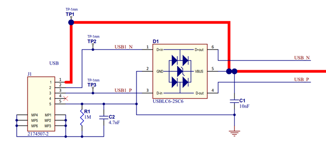
We have a nRF52820-QDAA-D-R7 on our 6-layer PCB with full ground layer beneath the chip. The chip has the external reset and SWD programming interface connected to test points for programming in a production test jig with no series resistors or decoupling capacitors attached. The chip also has an SPI interface for communication to a main MCU. Decoupling for VDD and DECx pins are according to datasheet recommendations. The external clock crystal is 32MHz and layout is according to datasheet recommendations. The BLE antenna interface is a matching filter with ground plane reference followed by a PCB antenna in top layer with cobber cut-outs in the other five layers (i.e. no ground plane reference). Layout and schematics can be provided upon request. Bluetooth communication is stable up to 30m indoor line-of-sight at 4dBm.
The BLE chip seems to be very susceptible to ESD discharges onto the shield of a micro-USB connector (only external interface) connected to PCBA ground. BLE connection is lost at ESD charges starting from 2KV air discharge to a metal ground reference sheet of 100pF (our ESD test bench setup). The main MCU (ATXMega family) seems unaffected - or at least significantly more robust to ESD discharges. When power-cycling the device, the BLE chip resets normally and is able to establish a new Bluetooth connection.
Do you have experiences with nRF52820 susceptibility to ESD and could you provide any design recommendations to reduce the sensitivity of the chip?
Best regards, Ivan Tving