Hello everyone,
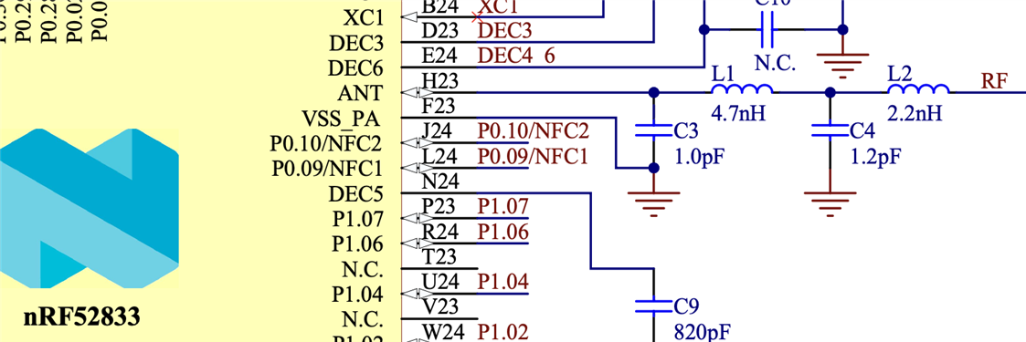
Currently I'm working on a specific BLE project so I have to design my own PCB, but basically I'm en embedded software engineer so I don't have deep knowledge when it come to PCB design. Therefore, I decided to opt to Nordic PCB design recommandation which is included in every chip product link. For example regarding the nRF52833 reference manual we can see that the RF feeding line LCL values are:
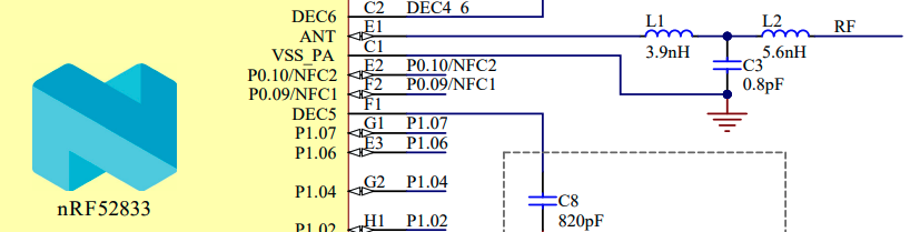
However, when Nordic team designed the development board for the same chip, they used different configuration for RF feeding line (you can get this by downloading the PCB desing of nRF52833 DK):

Here I've become confused since on one hand Nordic recommend to stick to the reference manuel settings and on the other hand Nordic team uses different configurations for the same chip.
And if the answer to this is "LCL circuit is antenna dependant", I would say that in the first example taken from the reference manuel there is no antenna so why would they specify specific values for the LCL circuit if there i no antenna ?
Please don't hesitate to share with me your knowledge about this topic, any information would be beneficial.
Thank you.
BR,
Bougrine Anis