Recommended External NFC antenna for nRF52840 Case ID: 322538

continue from previous closed ticket Case ID: 322538

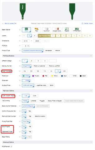
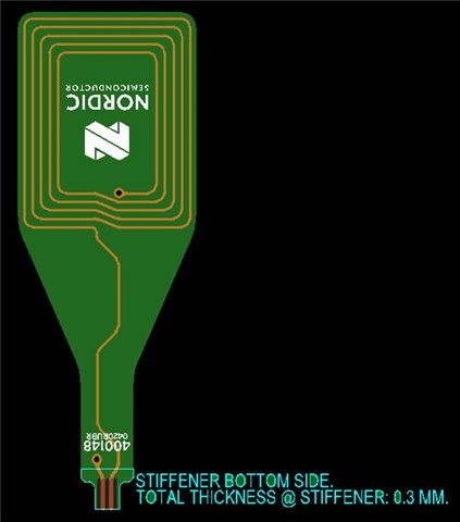
here i have recommended production file of nfc antenna from nordic semiconductor but the Gerber file does not include some confirmation which i get on jlc pcb while verification  

the above marked field is need to be verified by designed stackup and tested value but i haven't, for that i need assistance from expert "is this auto adapted values are right ?"

and in our another model i need to design nfc on pcb, where this reference design here, is key

here i need required impedance and recommended stackup for on board pcb nfc design.

thanks & regards 

  • Hi there,

    I see that your company have already made a case about this question here. My colleague is currently trying to find the answer on that question. Let's wait and see what he finds,

    regards
    Jared 

  • Yes, he is my colleague and is involved in this project as well. Let's see what progress they make.

    In the meantime, could you please guide me on designing an antenna on an FR4 PCB?

    Is it possible to simply copy and paste the existing design (even though my PCB has four layers and the existing antenna is on a two-layer flexible substrate)? If not, would you be able to help me design a new one and determine the appropriate board stackup? This would be most time-efficient for me.

    Thanks in advance for your assistance.

    Regards

  • Hi,

    Dhruvit said:
    Is it possible to simply copy and paste the existing design (even though my PCB has four layers and the existing antenna is on a two-layer flexible substrate)?

    Our development kit is a 4 layer board. You can probably copy our antenna that we use in our development kit reference design, but in the end you have to tune it to your specific board. An alternative would be to use a chip antenna instead such as the one we use in our Thingy series. If you have any further questions then I would advise you to create a new ticket as this is not related to your original question,

    regards

    Jared 

  • Hello, Jared 

    your colleague said "I don't have" , 

    and i also asked to jlc pcb for that required information they clearly said that " our gerber importer take automatic size and layers, other information need to be fill separately by user  "

    they also suggest me to get the designer to their website and fill the required information, where they specified important things like pcb thickness, gold thickness, gold fingers required thickness, polyimide thickness, emi shielding film required ground wirer. 

    if you can not able to find this information then suggest me a readymade product which you are giving with your DK board set. 

    because this is important thing in product certification.

    Thanks & Regards

  • Hi,

    You can try to contact Elprint and ask if they have the NFC antenna for sale. The order code at Elprint is 246803. 

    But if you decide to try to order the antenna from JLCPCB then you can use this design file:

    PCA64110-NFC antenna flexprint 1_0_1.zip

    And to answer this:

    ontinue from previous closed ticket Case ID: 322538

    here i have recommended production file of nfc antenna from nordic semiconductor but the Gerber file does not include some confirmation which i get on jlc pcb while verification  

    the above marked field is need to be verified by designed stackup and tested value but i haven't, for that i need assistance from expert "is this auto adapted values are right ?"

    • 2 layer Flex PCB
    • 0.05 mm thick with stiffener on connector side for a thickness of 0.3 mm
    • Dimensions: 58.8 mm x 21.3 mm
    • 1 oz copper
    • No gold fingers
    • No castellated holes


    regards

    Jared 

Related