Hi,
I want to develop a device using nRF52833. I am using QFN40, so can I use two UART connections. If yes, then what are the Tx, Rx pins for both the UART's
Hi,
I want to develop a device using nRF52833. I am using QFN40, so can I use two UART connections. If yes, then what are the Tx, Rx pins for both the UART's
Hi,
Yes, nRF52833 supports two UARTE instances (UARTE0 and UARTE1), as you can see in Registers. All nRF52 series chips has a pin crossbar feature, allowing any GPIO to be assigned to any serial peripheral like UART, SPI, TWI, etc. You should however avoid using pins marked as "Standard drive, low frequency I/O only" in Pin assignments for high frequency peripherals. The pins are controlled in FW, and both UARTE instances needs to be configured and initialized before use.
Best regards,
Jørgen
Hi,
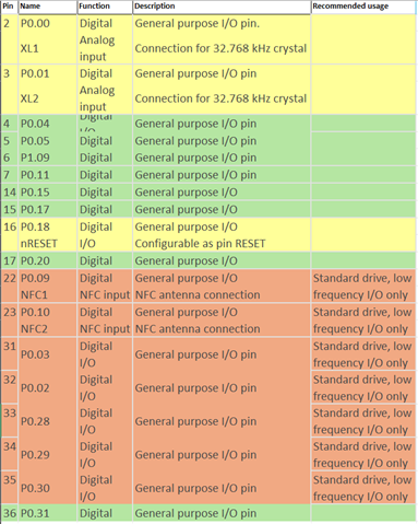
Like I said in my previous reply, ALL GPIOs can be assigned to the UARTs, but not all are recommended. Here is a table of available GPIOs on nRF52833 QFN40 package and their recommended usage:

Green shows GPIOs with no restriction. Red shows pins with frequency/drive restrictions, which should be avoided. I have also marked some pins in yellow. The yellow pins are shared with other functionality (32.768 kHz crystal pins and pin reset), so you might also want to avoid these pins if these functionalities are used in your product
Best regards,
Jørgen
What have you tried and what is not working? The chip comes blank from the factory and there is no other ways to do the initial programming of the chip than through the SWD pins.
Hi,
Can I use GPIO Standard drive, low frequency I/O for LED, Switch
Yes, as long as the switching frequency of the pin is below 10kHz and you do not draw large current from the pin (standard drive can source/sink a maximum of 1-4mA according to GPIO Electrical Specification).
what are the pins need to consider while i need to flash program from nRF52840 DK to external nRF52833 QDAA QFN40 SOC and share the procedure
Sai Mukesh said:what are the pins need to consider while i need to flash program from nRF52840 DK to external nRF52833 QDAA QFN40 SOC and share the procedure
Make the following connections:
The VTG/SWDIO/SWDCLK pins are available on P20 header on nRF52840 DK.
Sai Mukesh said:what are the pins need to consider while i need to flash program from nRF52840 DK to external nRF52833 QDAA QFN40 SOC and share the procedure
Make the following connections:
The VTG/SWDIO/SWDCLK pins are available on P20 header on nRF52840 DK.
as of know we dont had any soc but we had two development kits i.e. nRF52840 and nRF52833 both are DK's. now tried flashing the program form nRF52840DK of debug out (P20) to nRF52833DK debug in with help of 10pin bus cable .but we are facing the below issue
could please help us .
Flashing build_1 to 1050257546
C:\WINDOWS\system32\cmd.exe /d /s /c "west flash -d c:\Users\Pranathi\central_2\build_1 --skip-rebuild --dev-id 1050257546 --erase"
-- west flash: using runner nrfjprog
-- runners.nrfjprog: mass erase requested
-- runners.nrfjprog: Flashing file: c:\Users\Pranathi\central_2\build_1\zephyr\zephyr.hex
[error] [ Client] - Encountered error -102: Command read_device_info executed for 139 milliseconds with result -102
[error] [ Worker] - An unknown error.
[error] [ Client] - Encountered error -102: Command read_memory_descriptors executed for 31 milliseconds with result -102
Failed to read device memories.
[error] [ Worker] - An unknown error.
ERROR: JLinkARM DLL reported an error. Try again. If error condition
ERROR: persists, run the same command again with argument --log, contact Nordic
ERROR: Semiconductor and provide the generated log.log file to them.
NOTE: For additional output, try running again with logging enabled (--log).
NOTE: Any generated log error messages will be displayed.
FATAL ERROR: command exited with status 33: nrfjprog --program 'c:\Users\Pranathi\central_2\build_1\zephyr\zephyr.hex' --chiperase --verify -f NRF52 --snr 1050257546
The nRF52833 DK has its own built-in debugger, there should not be any need to program it from the nRF52840 DK, but it should be possible to program by connecting 10-pin cable between "Debug out" (P19) and "Debug in" (P18). You need to make sure both DKs are powered through the IMCU USB connector (J2) before programming.
Note that it is not possible to use P20 as debug input on the DKs.
we tried the same process but we are not able flash the program. do we need to do any changes in the firmware, we are using the vs code as ide so is there any specific changes needed or even though tried same with of on old nrf52833 soc but it also failed .please suggest any alternatives or step by step approach to follow
According to the documentation, when we short the SB47 solder bridge, it's supposed to prevent the internal System-on-Chip (SoC) from being detected and working. However, when we attempted to do this, we found that the program was still successfully flashed, and we were able to debug it.
This raises questions about why this happened and whether it might cause issues when flashing programs to external devices. Could you please clarify this matter for us? We want to ensure that everything is functioning correctly and avoid any potential problems.
On which DK did you short SB47? Have you verified that it is shorted properly?
Can you post a picture of your connections, and the logs from programming?
You can read out the register at address 0x10000100 to check which device is connected to the debugger:
nrfjprog --memrd 0x10000100
0x10000100: 00052833                              |3(..|