nRF5340 Soldering Issue

Hello,

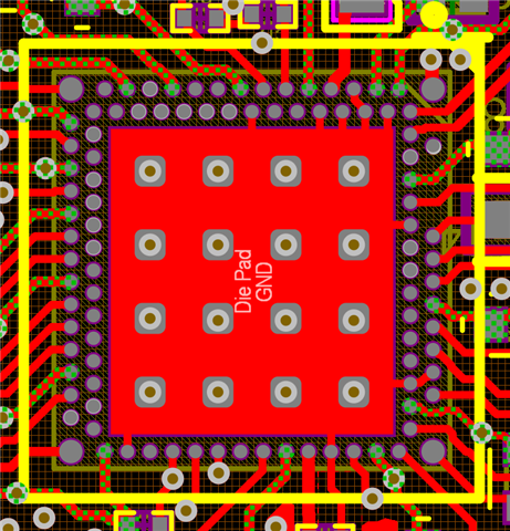
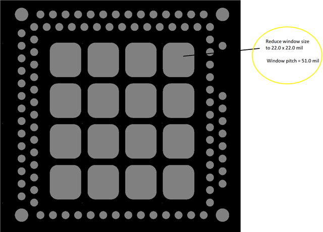
I am working on a custom PCB that involves the NRF5340 and our first iteration of PCBs had soldering issues during assembly for the nRF5340. The nRF5340’s footprint in my design is copied from the example footprint given by Nordic. I asked the production team we are working with about the soldering issue and they said, "The problem was the solder paste deposition on the ground pad was a bit excessive which caused the chip to float up during reflow and leaving a gap between the PCB land and the chip signal pads. Thus, poor solder joints occurred.” They suggested shrinking the die pad’s paste windows as in the image below. The picture is the Nordic example footprint’s Top Paste layer in Altium and the bubble is their suggestion.


Is there any reason we should not shrink the window size in the Top Paste layer? Does anyone have any suggestions on changing the paste layer to make sure we do not have soldering issues again?

Parents
  • After looking through the application notes mentioned by Simonr and reviewing the Nordic footprint example, I have finished with this as a final set up (22milx22mil solder paste windows and 8mil diameter thermal via holes):

    One item that I noticed was changed by another designer on my team was the size of the thermal via holes in the die pad. He had changed them to be 8mil diameter holes instead of the default 12mil diameter holes. Could the holes being shrunk be the reason for the default solder paste windows leaving too much solder and causing assembly issues? Does anyone see a reason why leaving the thermal vias smaller and making the solder paste windows smaller to compensate would be an issue?

Reply
  • After looking through the application notes mentioned by Simonr and reviewing the Nordic footprint example, I have finished with this as a final set up (22milx22mil solder paste windows and 8mil diameter thermal via holes):

    One item that I noticed was changed by another designer on my team was the size of the thermal via holes in the die pad. He had changed them to be 8mil diameter holes instead of the default 12mil diameter holes. Could the holes being shrunk be the reason for the default solder paste windows leaving too much solder and causing assembly issues? Does anyone see a reason why leaving the thermal vias smaller and making the solder paste windows smaller to compensate would be an issue?

Children
No Data
Related