ADC Noise in 2 successive reads from different channels

Dear Nordic Semiconductor Support,

We are experiencing an issue with our NRF52832 chip while performing ADC reads in a Zephyr environment. Our setup involves two ADC channels: AIN2 for battery voltage and AIN3 for a Force-Sensing Resistor (FSR). The FSR is sampled more frequently than the battery voltage.

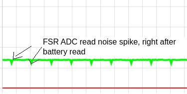
When we perform a battery voltage read on AIN2, the subsequent FSR sample on AIN3 contains significant noise. If we discard the first sample after the battery read, subsequent FSR samples return to normal levels. If the battery voltage ADC reads are not performed, the noise issues in the FSR reads are not observed, this issue does not occur if the battery voltage reading is disabled.


Could you please provide insights or suggestions on how to resolve this noise interference between the two ADC channels? Any recommendations for ADC configuration settings or sequencing that might mitigate this issue would be greatly appreciated.

Best regards,
Pedro

  • ADC channel-to-channel performance is affected by timing and the starting source prior to a specific channel measurement; longer settle (aka sampling) time reduces somewhat but does not eliminate the starting source. By starting source I mean the voltage on the internal ADC prior to selecting the new voltage. Often this can be optimised by simply reading a fixed known starting source prior to every ADC channel read, most often GND. Better, take that GND measurement and use it as an offset to be subtracted from the actual channel; this is a technique known as Correlated Double Sampling (CDS), widely used with photodiode sensors.

    Try this sampling sequence to get over the problem: GND - AIN2 - GND - AIN3 - AIN3 - AIN3 - AIN3 ...

    or - cleaner: GND - AIN2 - GND - AIN3 - GND - AIN3 ...

    A second consideration is to physically separate the ADC input pins either with or without a GND channel; ie use AIN1 and AIN3, even better set AIN0 and AIN2 to GND if there are enough spare pins and use those two GNDs as the starting point to measure the two required voltages..

  • Thanks for the insightful reply  !
    For implementing the suggested GND sampling, should one of the ADC channels be configured to connect directly to GND, or is there another internal method I could use without dedicating a channel for this?

  • Regrettably no, only VDD; VDD could be used but there is likely to be more interference from VDD than GND. The internal pull-down bias resistor could be used to hold a spare analogue channel at GND without using an external board modification, but better results would be obtained by using a GND related to the measurement itself ie the GND end of the FSR circuit. Internal ADC GND is subtly different in any case: "The assumption in single-ended mode is that the internal ground of the ADC is the same as the external ground that the measured voltage is referred to. The ADC is thus sensitive to ground bounce on the PCB in single-ended mode. If this is a concern we recommend using differential measurement." This is why differential measurements between a single-ended signal and a related GND are usually less noisy than single-ended measurements with internal GND as the negative input. The external GND ADC channel could be shared between both signals battery and FSR; it serves a dual purpose, repeatable start point and CDS.

Related