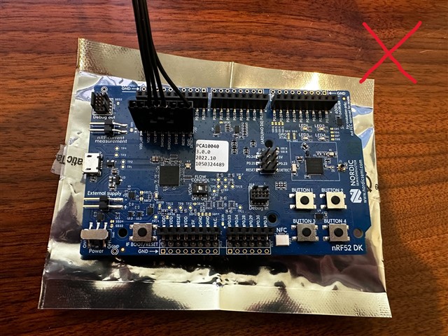
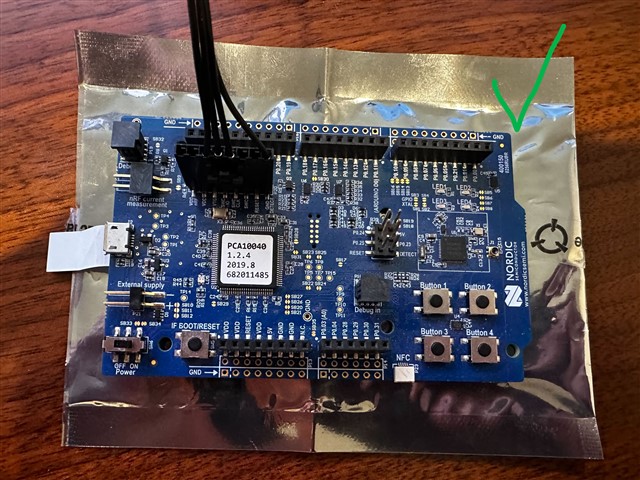
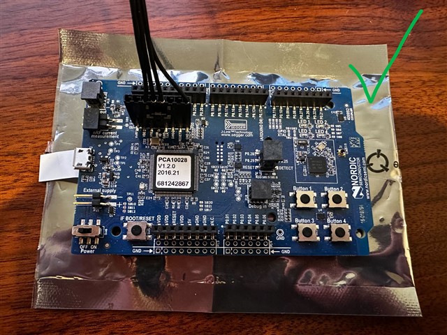
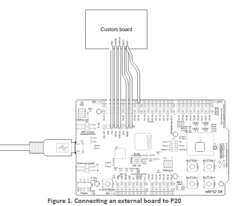
I'm running into issues with programming external boards (an NRF52832_xxAA_REV2, an NRF52810_xxAA_REV2, an NRF51xxx_xxAC_REV3, and an NRF52832_xxAA_REV3) through a custom connector on an nRF52 DK that uses the J-Link OB-nRF5340 and can't figure out what's going wrong, This only seems to be a problem with the nRF5340 programmer (PCA10040 Rev 3.0.0), because I have two dev kits with an older J-Link programmer (PCA10040 Rev 1.2.4 & PCA10028 Rev 1.2.0) that work just fine.
Here's how I have the connector hooked up (which I found at https://infocenter.nordicsemi.com/index.jsp?topic=%2Fug_nrf52832_dk%2FUG%2Fdk%2Frevision_history.html)
I'm using J-Link v7.96f (though I've also tried this with v7.94f and the results are the same)
The J-Link OB-nRF5340 is running the 4/11/24 firmware: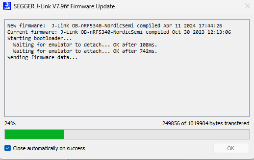
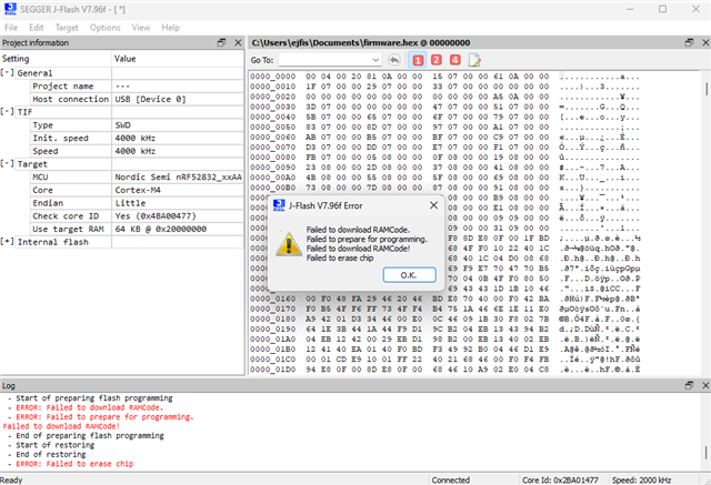
When using nRF Connect for Desktop (v4.4.1) Programmer (v4.3.0) to program the device (for example the NRF52832_xxAA_REV2) through the DK with the J-Link nRF5340, after clicking "Erase all", loading my firmware file, and hitting "Erase & write" I get these errors:
SEGGER J-Link Commander V7.96f (Compiled Apr 24 2024 14:14:02)
DLL version V7.96f, compiled Apr 24 2024 14:13:07
Connecting to J-Link via USB...O.K.
Firmware: J-Link OB-nRF5340-NordicSemi compiled Apr 11 2024 17:44:26
Hardware version: V1.00
J-Link uptime (since boot): 0d 00h 07m 24s
S/N: 1050324489
License(s): RDI, FlashBP, FlashDL, JFlash, GDB
USB speed mode: Full speed (12 MBit/s)
VTref=3.300V
Type "connect" to establish a target connection, '?' for help
J-Link>device NRF52
J-Link>si SWD
Selecting SWD as current target interface.
J-Link>speed 4000
Selecting 4000 kHz as target interface speed
J-Link>connect
Device "NRF52" selected.
Connecting to target via SWD
InitTarget() start
InitTarget() end - Took 2.68ms
Found SW-DP with ID 0x2BA01477
DPIDR: 0x2BA01477
CoreSight SoC-400 or earlier
Scanning AP map to find all available APs
AP[2]: Stopped AP scan as end of AP map has been reached
AP[0]: AHB-AP (IDR: 0x24770011)
AP[1]: JTAG-AP (IDR: 0x02880000)
Iterating through AP map to find AHB-AP to use
AP[0]: Core found
AP[0]: AHB-AP ROM base: 0xE00FF000
CPUID register: 0x410FC241. Implementer code: 0x41 (ARM)
Found Cortex-M4 r0p1, Little endian.
FPUnit: 6 code (BP) slots and 2 literal slots
CoreSight components:
ROMTbl[0] @ E00FF000
[0][0]: E000E000 CID B105E00D PID 000BB00C SCS-M7
[0][1]: E0001000 CID B105E00D PID 003BB002 DWT
[0][2]: E0002000 CID B105E00D PID 002BB003 FPB
[0][3]: E0000000 CID B105E00D PID 003BB001 ITM
[0][4]: E0040000 CID B105900D PID 000BB9A1 TPIU
[0][5]: E0041000 CID B105900D PID 000BB925 ETM
Memory zones:
Zone: "Default" Description: Default access mode
Cortex-M4 identified.
J-Link>erase
No address range specified, 'Erase Chip' will be executed
'erase': Performing implicit reset & halt of MCU.
Reset: Halt core after reset via DEMCR.VC_CORERESET.
Reset: Reset device via AIRCR.SYSRESETREQ.
Reset: CPU may have not been reset (DHCSR.S_RESET_ST never gets set).
Reset: Using fallback: Reset pin.
Reset: Halt core after reset via DEMCR.VC_CORERESET.
Reset: Reset device via reset pin
Erasing device...
****** Error: Verification of RAMCode failed @ address 0x2000041C.
Write: 0x481CF815 D3024284
Read: 0x481CF895 D3024284
Failed to prepare for programming.
Failed to download RAMCode!
ERROR: Erase returned with error code -1.
J-Link>loadfile "C:\Users\ejfis\Documents\firmware.hex"
'loadfile': Performing implicit reset & halt of MCU.
Reset: Halt core after reset via DEMCR.VC_CORERESET.
Reset: Reset device via AIRCR.SYSRESETREQ.
Downloading file [C:\Users\ejfis\Documents\firmware.hex]...
****** Error: Verification of RAMCode failed @ address 0x2000021C.
Write: 0x9400E00C 002A003B
Read: 0x9400F00C 002A003B
Failed to prepare for programming.
Failed to download RAMCode!
Unspecified error -1
The same thing happens when using the actual J-Link v7.96f JFlash.exe program: