nRF52840 Custom PCB Design

Hi,

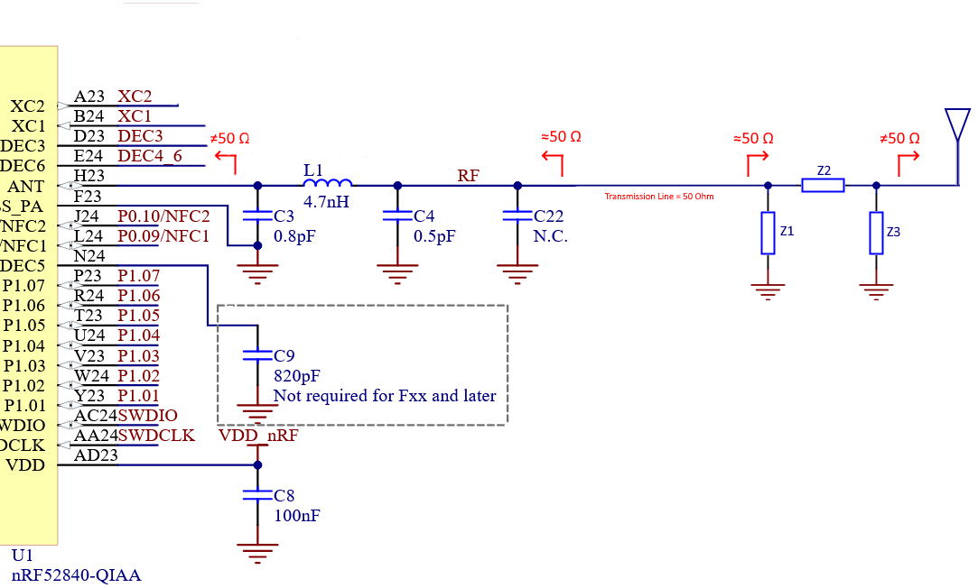
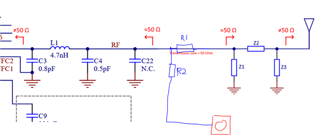
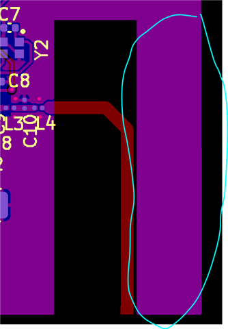
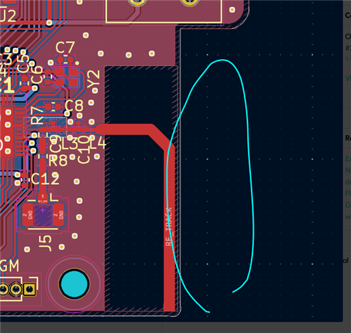
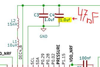
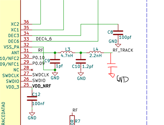
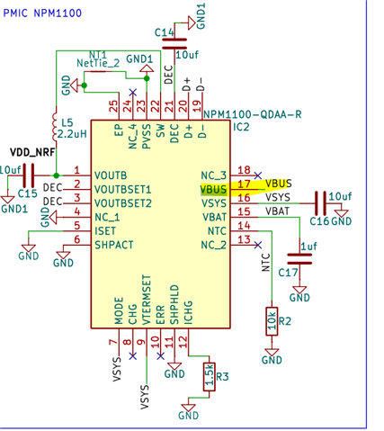
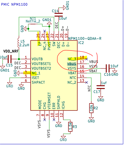
I am designing a two Layer PCB with nRF52840 with PMIC, RTC, Flash. Can anyone from Nordic Review it? especially the RF antenna, I have used the Reference design from Nordic, since it is an RF circuit its my first time doing it. My current design has both a track antenna and UFL connector. I am Attaching all the required files below.

Gerber Files: OUTPUT.rar
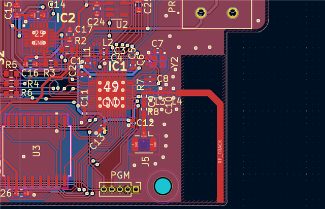
Thankyou

Parents
  • Hello!

    Yes we do reviews and will happily provide feedback and help with what we can.

    Here is the feedback:

    You have misunderstood what matching network is required for the antenna and not. 

    The ANT pin on the SoC is not matched to 50 Ohms so it needs a matching network. This is what I like to call the radio matching components, it does two things, firstly it matches the output from the ANT pin to what will be the transmission line at around 50 Ohms, Secondly it suppresses the harmonics so it acts like a filter. 

    Here is a simpler typical schematic for what we recommend in most cases.

    The Z1,Z2 and Z3 components here are specifically for the antenna ant to match and tune it. The first components here
    C22 can be removed. 


    So you would want to add you connector after the C4 component in the image above. something like this:


    For PCB antennas like the one you have a single shunt caps will often be good enough to tune the antenna if also the antenna length is adjusted correctly. 


    Layout looks mostly ok, there are some of the above mentioned things that needs to change but otherwise ok. 
    GERBER files show some major copper area in a place the image does not show, 

    Just want to not that that should not be there as it will effect antenna performance. 


    So looks ok here in this image. 


    Would be nice to see the schematic and check that all the values are correct. 


    We have some resources here: 
    https://devzone.nordicsemi.com/guides/hardware-design-test-and-measuring/b/nrf5x/posts/general-pcb-design-guidelines-for-nrf52-series 


    Video here: 

    PCB Antenna - How To Design, Measure And Tune 


    You can directly upload files here as well, no need to create a link if you don't want to. 

    Regards,
    Jonathan

  • Thankyou Jonathan for the fast response. 

    single shunt caps will often be good enough to tune the antenna if also the antenna length is adjusted correctly.

    In My design, I have my Antenna Length as 23mm what should be the shunt capacitor value?.I will share my schematic here.

    NRF52840_TEST.pdf

    Thanks.

  • Shabinkumar said:
    I have my Antenna Length as 23mm what should be the shunt capacitor value?.I will share my schematic here.

    It is very difficult to give you the value with just the data from schematic\layout files. Only way to properly get the correct value is to do the tuning with a VNA, looking at the antenna and testing with a couple different values. 

    We do provide tuning services here at Nordic, so if you want you ca send a device to us and we will tune it for you and provide a list of values that gives the best results. 


    Schematic review:

    Should be 47nF not 1uF. 


    Should add at least one shunt close to the antenna


    VBUS has no decupling from what i can see in the schematic


    PIN 18 can also be connected to VSS\GND. 


    Regards,
    Jonathan

Reply
  • Shabinkumar said:
    I have my Antenna Length as 23mm what should be the shunt capacitor value?.I will share my schematic here.

    It is very difficult to give you the value with just the data from schematic\layout files. Only way to properly get the correct value is to do the tuning with a VNA, looking at the antenna and testing with a couple different values. 

    We do provide tuning services here at Nordic, so if you want you ca send a device to us and we will tune it for you and provide a list of values that gives the best results. 


    Schematic review:

    Should be 47nF not 1uF. 


    Should add at least one shunt close to the antenna


    VBUS has no decupling from what i can see in the schematic


    PIN 18 can also be connected to VSS\GND. 


    Regards,
    Jonathan

Children
No Data
Related