Dear nRF Support Team and Community Members,
I hope this message finds you well. I am currently working on a low power wearable electronics project. This is my first attempt at designing a four-layer PCB using Altium software, and I would greatly appreciate your expert review and feedback on my design.
Project Overview:
- Project Name: Low Power Wearable Device (LPWD)
- Objective: To develop a low power wearable device aimed at health monitoring applications.
- Key Features:
- BLE (Bluetooth Low Energy) connectivity using nRF52840
- Integrated sensors:
- Accelerometer: BMA400
- Humidity and Temperature: HTS221
- Pressure: LPS22HH
- Color: BH1749
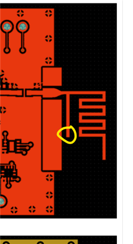
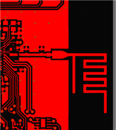
- Recommended antenna: AN91445
- Target Power Consumption: 1-5mW
Files for Review:
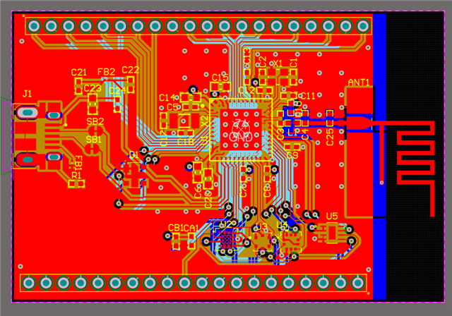
- Schematic: Schematic of LPWD.pdf
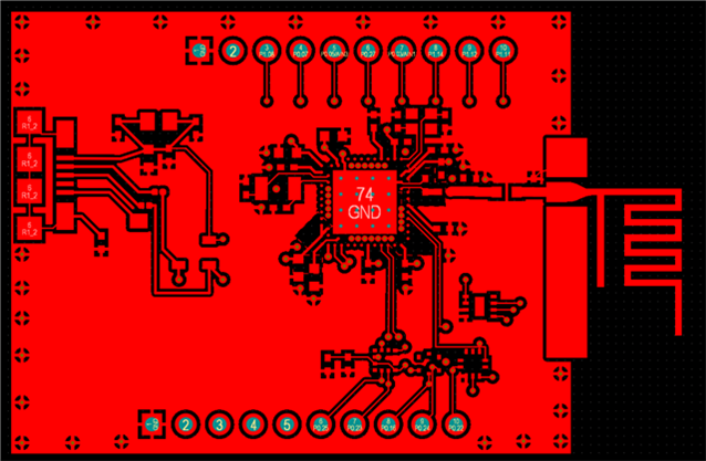
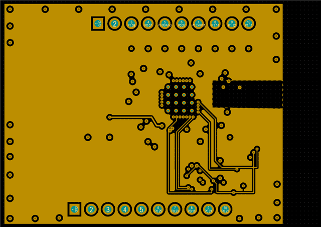
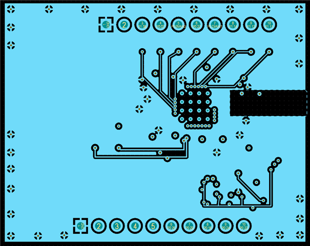
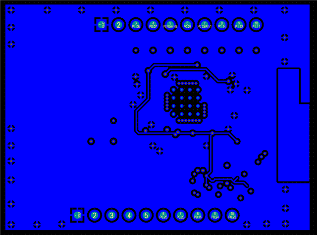
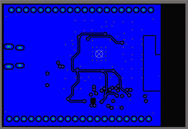
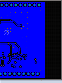
- Gerber Files: Gerber of LPWD.zip
Areas of Concern:
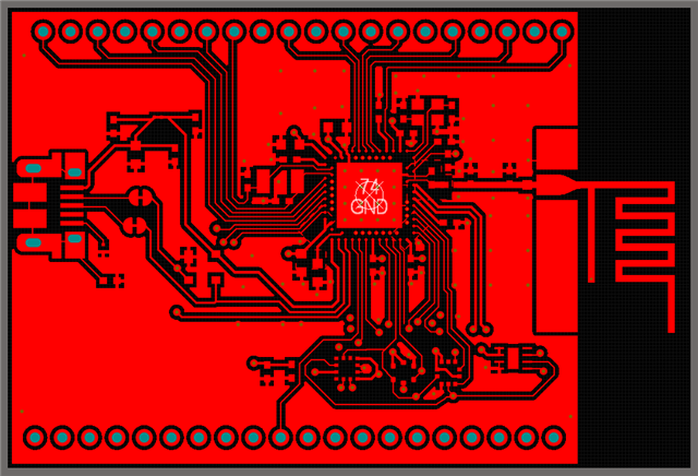
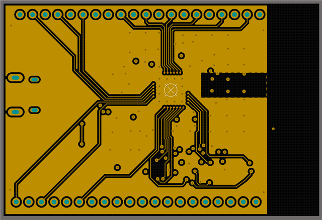
- Pin Assignments: Verification of correct pin assignments and connections for the nRF52840 and sensors.
- Component Values: Validation of passive component values and their suitability for the circuit.
- Power Management: Assessment of the power management circuitry for potential issues and efficiency.
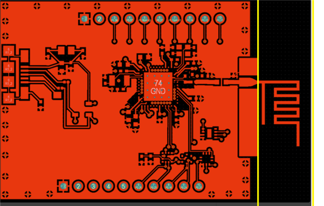
- RF Layout: Review of the RF section, including the antenna, to ensure optimal signal integrity and performance.
- Overall Layout: General feedback on the PCB layout and routing, particularly with respect to signal integrity and power distribution.
- Sensor Integration: Proper integration and placement of the accelerometer, humidity and temperature sensor, pressure sensor, and color sensor.
Additional Information:
- The design aims to minimize power consumption while maintaining reliable operation of the sensors and BLE communication.
- Ensuring good RF performance and low noise is critical for this wearable device.
I have attached the schematic in PDF format and a ZIP file containing the Gerber files for your convenience. Your insights and feedback will be invaluable to ensure the robustness and reliability of this design.
Thank you in advance for your time and assistance. I look forward to your expert guidance.