Hi community,
It's my first time building a board with a Nordic chip so for sure I've made a lot of mistakes. I made this with KiCad and uploaded all the files to the repository:
https://github.com/martinberlin/Sharp-LV | Schematics here: https://github.com/martinberlin/Sharp-LV/blob/main/Sharp-LV-schematic_Rev1.0.pdf (Just hit the download button to see it well)
I've got some Nordic nRF52 boards from chinese firma Seeed that worked very well so I'm tempted to make my first open-source PCB.
Unique goal of this first revision 1.0:
- To drive the display and be able to flash it using USB-C that's the only wish for 1st release. All the rest including Bluetooth RF is secondary.
QUESTIONS
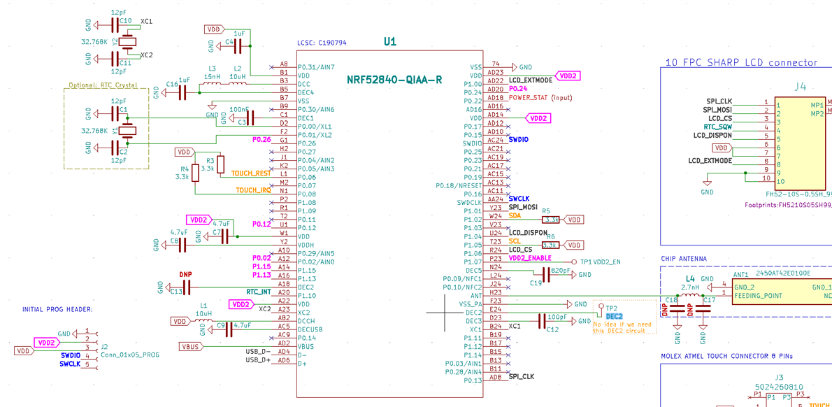
- I could not find any specific document specifying what are the DEC** pins. So I've based my design on looking at the Schematics of other boards I've found online,
As an example I left DEC2 unconnected just to a test point since in some designs was not used, in others yes, so I was not sure what is the right setup - Is this board very sensible with the RF tunning? I ask since I know Espressif S3 is for example and might get hot if you don't make the right layout (I do not have an electronic laboratory at home, so no special tools to "tune" RF)
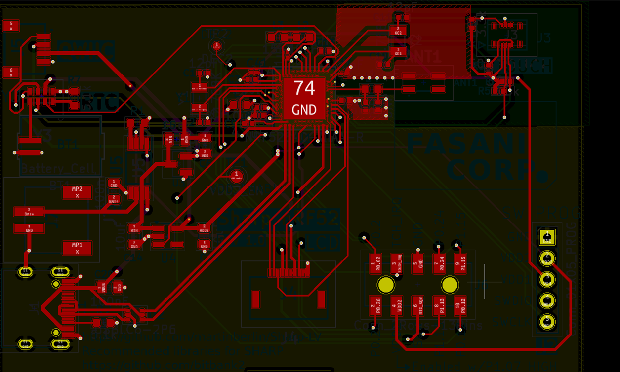
A small preview of how the KiCad 4 layers of the PCB look like:
Fcu
In2: /resized-image/__size/640x480/__key/communityserver-discussions-components-files/4/In2.png
Bcu:
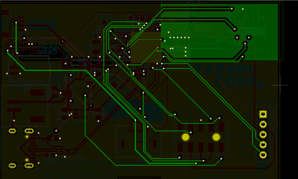
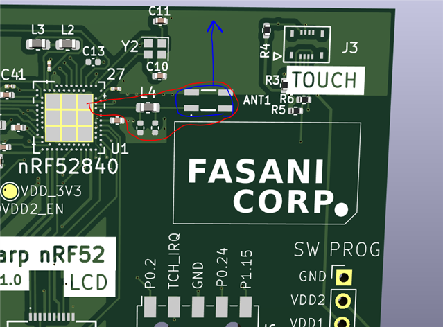
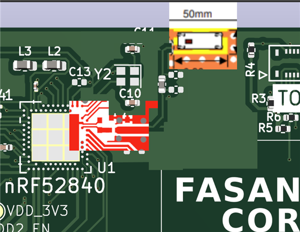
RF antenna: https://www.lcsc.com/product-detail/Antennas_Johanson-Dielectrics-2450AT42E0100E_C3285081.html it worked for me correctly in another Espressif boards I've designed. Just badly tuned since I've mentioned before I lack the knowledge and tools to "tune correctly" an Antenna. Not to mention RF is just a whole world in itself!!!
Anyways my whole point on writing this is to get a "schematics review" of peers that have a lot more experience than me and can point to some obvious details. Thanks a lot for reading this and hopefully I can get my first PCB with Nordic working

