Schematics sanity check for a Sharp LCD controller using NRF52840

Hi community,

It's my first time building a board with a Nordic chip so for sure I've made a lot of mistakes. I made this with KiCad and uploaded all the files to the repository:

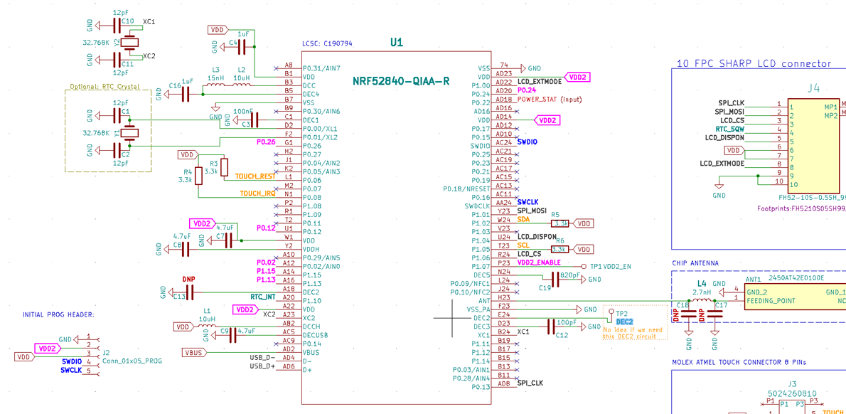
https://github.com/martinberlin/Sharp-LV     | Schematics here: https://github.com/martinberlin/Sharp-LV/blob/main/Sharp-LV-schematic_Rev1.0.pdf (Just hit the download button to see it well)

I've got some Nordic nRF52 boards from chinese firma Seeed that worked very well so I'm tempted to make my first open-source PCB.

Unique goal of this first revision 1.0:

  1. To drive the display and be able to flash it using USB-C that's the only wish for 1st release. All the rest including Bluetooth RF is secondary.

QUESTIONS

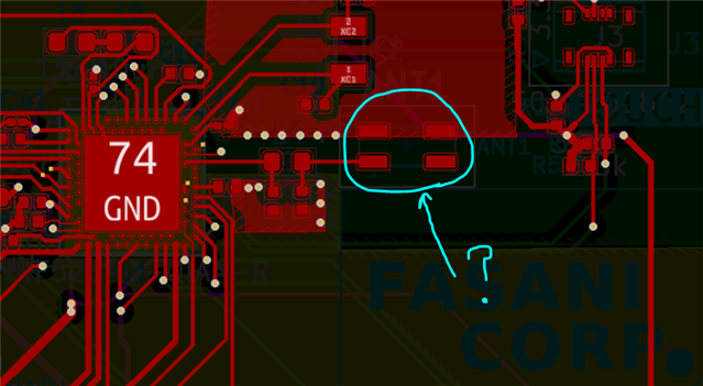
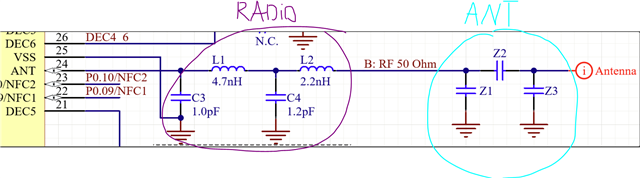
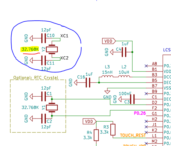
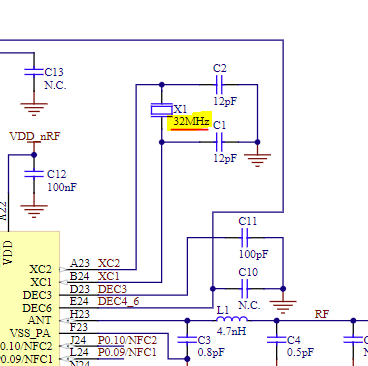
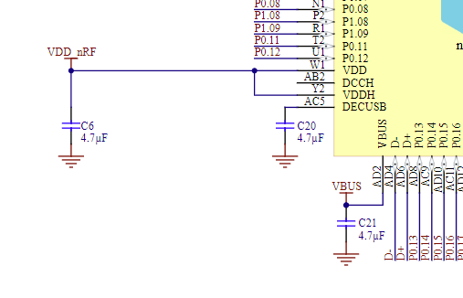
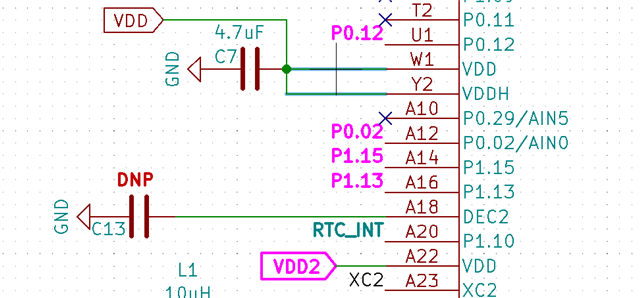
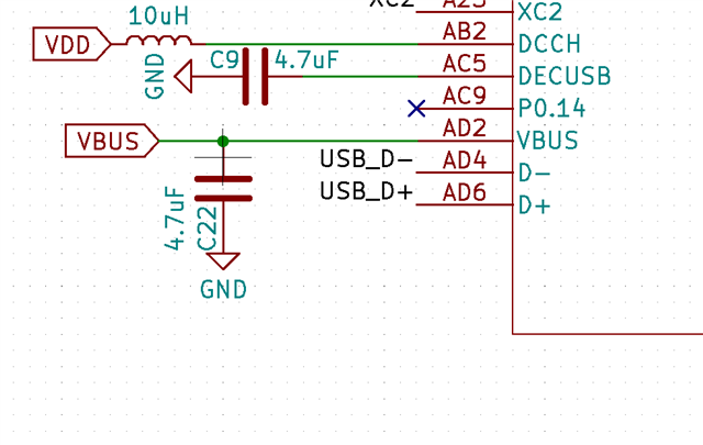
  1. I could not find any specific document specifying what are the DEC** pins. So I've based my design on looking at the Schematics of other boards I've found online,
    As an example I left DEC2 unconnected just to a test point since in some designs was not used, in others yes, so I was not sure what is the right setup
  2. Is this board very sensible with the RF tunning? I ask since I know Espressif S3 is for example and might get hot if you don't make the right layout (I do not have an electronic laboratory at home, so no special tools to "tune" RF)

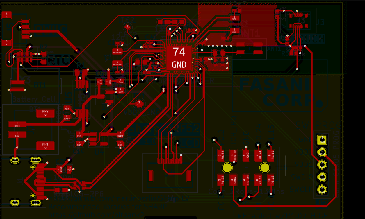
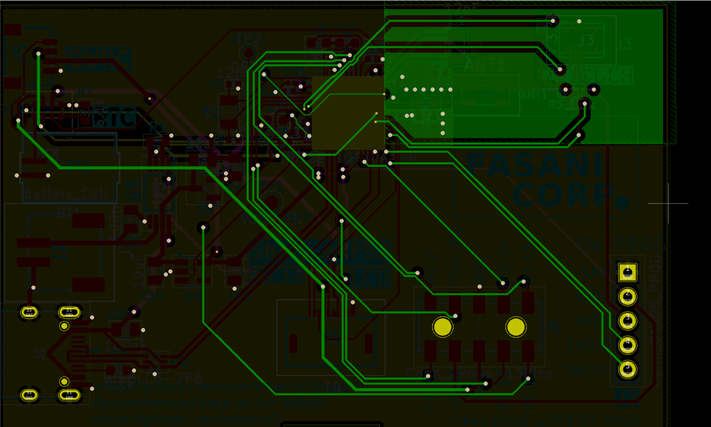
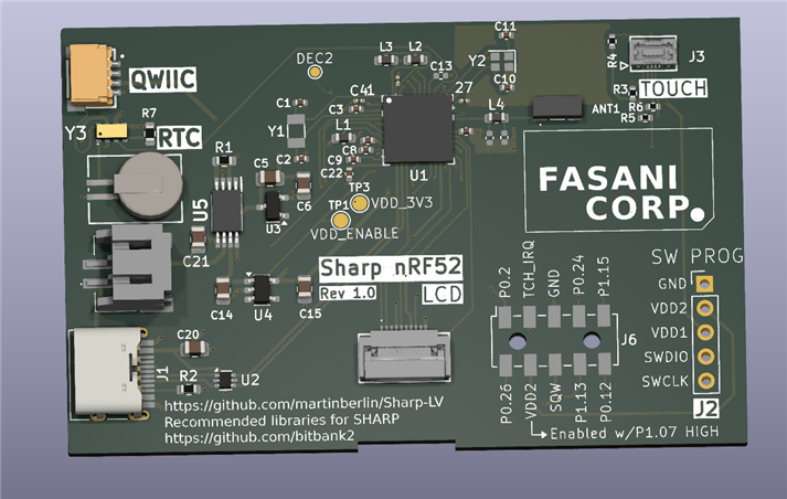
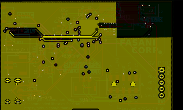
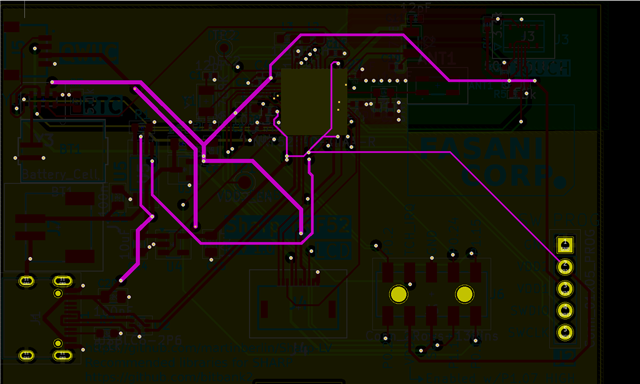
A small preview of how the KiCad 4 layers of the PCB look like:
Fcu


In1: ttps://devzone.nordicsemi.com/resized-image/__size/640x480/__key/communityserver-discussions-components-files/4/In1.png

In2: /resized-image/__size/640x480/__key/communityserver-discussions-components-files/4/In2.png

Bcu:

RF antenna: https://www.lcsc.com/product-detail/Antennas_Johanson-Dielectrics-2450AT42E0100E_C3285081.html it worked for me correctly in another Espressif boards I've designed. Just badly tuned since I've mentioned before I lack the knowledge and tools to "tune correctly" an Antenna. Not to mention RF is just a whole world in itself!!!

Anyways my whole point on writing this is to get a "schematics review" of peers that have a lot more experience than me and can point to some obvious details. Thanks a lot for reading this and hopefully I can get my first PCB with Nordic working

  • Update found nRF52 RF Guidelines here:  General PCB design guidelines for nRF52 series   
    For a first release maybe it will be the safest to go for that, just copy the reference design!
    I just need to check if I can import it in KiCad

  • Dont think KiCad supports importing Altium files currently.


    But try to copy the layout as best you can, we do provide the GERBER files that you can also use as a reference. 

    There is also a video going through some details that you might find useful. 

    PCB Antenna - How To Design, Measure And Tune


    To drive the display and be able to flash it using USB-C that's the only wish for 1st release. All the rest including Bluetooth RF is secondary.

    You would need a pre-flashed SoC with a bootloader on it to be able to flash over USB(-C), If you have a new SoC strait from the factory installed on you custom PCB you will need to program it over the SWD interface pins first and flash a bootloader to it before flashing over USB will work. Nordic dont sell any SoC with preinstalled software\firmware. 


    Antenna placment:
      

    So it looks like you have placed the antenna in the "middle" of PCB, that is not good if you want to have long range. If you have a look in the datasheet of this antenna you can see that is is recommended to have it placed on the edge. Its always best to follow the antenna manufacturers recommendation for best results. 


    Also its recommended to have its own matching components, so the antenna should have its own little network of a couple components to be able to tune it properly.


    So both the Radio (the components closest to the ANT pin on the SoC) and the Antenna should have its own matching network. 


    Also you have the wrong Crystal for XC1\XC2, you have mounted a 32kHz for both crystals, this is wrong and will not work. You need a 32MHz crystal.


    For power it looks like you are using a 3.3V regulator so you can keep to the simplest normal voltage mode design: Where VDD and VDDH is connected like seen in ref design config 5.  

    You can also add the 4.7uF cap to VBUS pin as well. You all ready have the DECUSB cap correct. 


    Feel free to ask more questions or update when you have done some changes and want some more feedback 

    Regards,
    Jonathan

  • Thanks for your great review Jonathan. Great catch about the RTC "Clock" (I was probably thinking on that crystals)

    Will switch them to the right ones. All the other tips where also super helpful. Will update this over the weekend and make the required changes

  • Happy to help!

    Thanks a lot for reading this and hopefully I can get my first PCB with Nordic working

    Will get you all the way there

    Regards,
    Jonathan

  • You would need a pre-flashed SoC with a bootloader on it to be able to flash over USB(-C), If you have a new SoC strait from the factory installed on you custom PCB you will need to program it over the SWD interface pins first and flash a bootloader to it before flashing over USB will work. Nordic dont sell any SoC with preinstalled software\firmware. 

    Understood. I added there SW headers and have around in the studio one adapter that I've used to flash STM32 chips in the past.
    Updated schematics in this new PDF so it's possible to compare with the old one linked at the beginning:
    https://github.com/martinberlin/Sharp-LV/blob/main/SharpLV-schematics_1.0.pdf

    > Also you have the wrong Crystal for XC1\XC2, you have mounted a 32kHz for both crystals, this is wrong and will not work. You need a 32MHz crystal.

    Great catch now this is updated by a 32 Mhz crystal, that was provided by a colleague that did another Nordic board that is proved to work (https://github.com/mike-rankin/nRF52832_Oled_Board)
    Replaced this crystal with LCSC part nr: C409316


    > For power it looks like you are using a 3.3V regulator so you can keep to the simplest normal voltage mode design: Where VDD and VDDH is connected like seen in ref design config 5.

    Corrected thanks for the tip.


    This is also make me re-think the idea of having 2 sources of VDD (Main & Vdd2) that I was supposed to turn on once the MCU awakes and that will also power external peripherals. I thought could be a good idea to check consumption and see if it could help in some parts to keep only MCU powered and all the rest off. But for a 1st design is a too complicated idea and I'm thinking to get rid of it.

    > You can also add the 4.7uF cap to VBUS pin as well. You all ready have the DECUSB cap correct. 

    Added.


    Y2 is the new 32 Mhz Crystal. C22 is the 4.7 uF CAP to VBUS 5v.

Related