Good Afternoon,
I'm designing a 4-layer PCB based on an NRF52832 (QFAA) paired wit h a Molex 479480001 SMT Antenna, and I was hoping for some feedback on Antenna Matching.
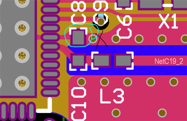
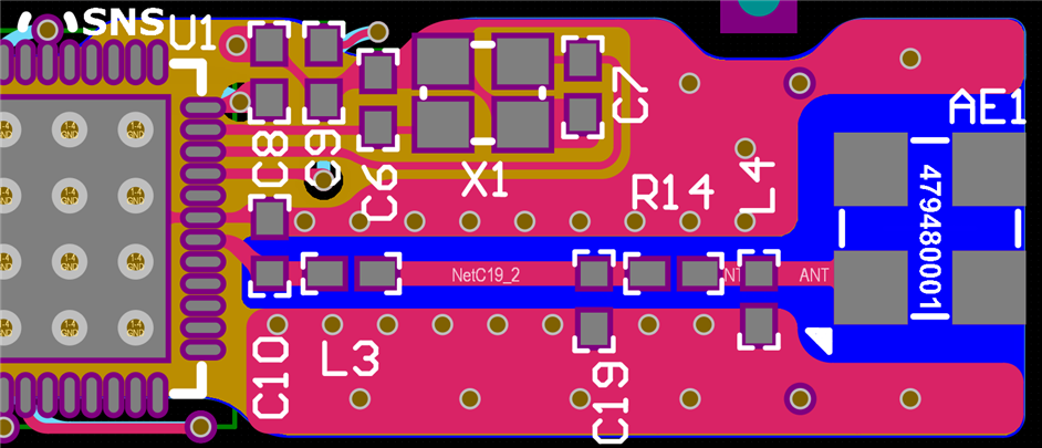
Here's a partial screenshot of the current layout, followed by the associated schematic:
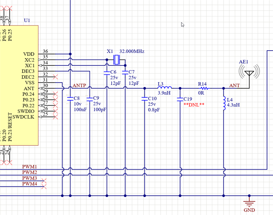
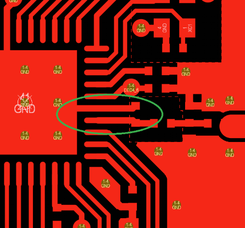
As per the application notes of the nrf52832 (QFAA footprint), I've including an 0.8pF Capacitor (C10) and 3.9nH Inductor (L3) for matching at the output of the IC. There's what I hope is a reasonable approximation of a coplanar waveguide on the PCB, with trace width adjusted to match my layer stack-up and PCB fab specs.
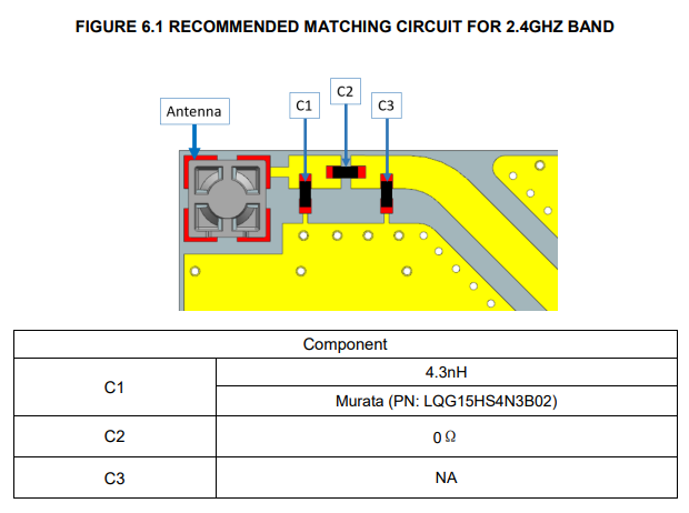
As per the Application Note of the Molex antenna, I've added a 0R jumper (R14), 4.3nH inductor (L4) and optional capacitor (C9) close to the antenna:
Are there any glaring mistakes here, or anything I can do to further improve the design in terms of RF performance, prior to sending the PCB out for fabrication?
Thank you very much!