nRF52833, GPIO default states Post Power OFF and NOT System Off mode

Hello,

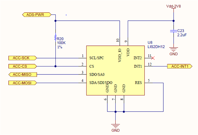
Our nRF52833 is powered through a load switch and control when to enable it is based on external peripherals logic. The MCU is connected to external peripherals that are ALWAYS powered ON and I am seeing what I think is leakage back into the MCU as I am measuring approx. 0.3V on the MCU coupling caps when its powered OFF. The MCU is connected to external IMU, EEPROM Memory, low power Accelerometers, and Hall sensors. All these external peripherals are connected via SPIM buses. Again, some of these are ALWAYS powered ON and some are only ON while the MCU is ON.  the peripherals that are NOT always ON are also controlled via a load switch and their enable pin is controlled by the nRF52833. 

I need to make sure the enable pin on the load switches of those peripherals that are disabled when the MCU is powered down are NOT floating. I do not want to use an external pull-down resistor as that would dramatically increase my power consumption when operating that sensor.

My question is: will the nRF52833 internal pull-downs remain when its load switch is DISABLED(no power going to it) as in the "system OFF mode" outlined in the datasheet?

also, any input on what happens to the peripherals that are always powered ON but their CS pin is either floating or pulled down as would be the case in this scenario when they operate on SPI Mode 0(CS is active when pulled low)? 

In sum, power is my main concern and even placing 10M ohms pull downs is not sufficient for my design case.

your help will be greatly appreciated. 

Regards,

Wael

Parents
  • Hello Wagel,

    ''I need to make sure the enable pin on the load switches of those peripherals that are disabled when the MCU is powered down are NOT floating'' 

    If the MCU is powered down, then GPIO pin will not get any power, in this case default configuration of pulled down register will not work. You need to cntrol the GPIO externally.

    Thanks.

    BR

    kazi

  • hi kazi,


    Thank you for your reply. That was my assumption but I am actually experiencing the opposite. where if I configure the GPIO pin with pulldowns prior to powering the MCU OFF, the enable signal seems to be kept low/pulled down. if I don't configure the pin that way, the load switch that the GPIO controls is enabled. How can you explain that? Your help is greatly appreciated.

  • If I may comment as an outsider, the reset function will generally not work correctly when nRF52 VDD power is removed and the voltage allowed to slowly sink as the bulk capacitance on nRF52 VDD discharges as any output pin on the connected external peripherals will back-drive (phantom power) nRF52 VDD through the internal schottky diodes to VDD within the nRF52. The effect of this is the reset does not happen as expected, and the port pin settings are not therefore cleared to defaults. The solution is to isolate any external peripheral output pins which connect to the nRF52 with a level translator (aka buffer) whose logic supply is connected to nRF52 VDD and not the external peripheral VDD. I use a SN74LV1T34DCKR for this purpose, one on each external peripheral output pin connecting to the nRF52; these are available in multiple buffers/package. Other solutions, such as series resistors, are unsafe. A separate consequence of not using buffers is the nRF52 may or may not behave on restoration of nRF52 VDD. An alternative solution is to simply drive low or float all external peripheral output pins driving the nRF52 prior to turning off nRF52 VDD, not always possible depending on the hardware.

  • hello hmolesworth,

    Thank you for you response! I have few questions and I am hopping you may be able to shed some light on them.

    1) The external peripherals connected to nRF52 when its powered OFF are the following

    - a low power accelerator. it has the SPI lines and one active-high interrupt pin. Since the SPI lines are controlled by the nRF52 and the interrupt pin is an active-high ensuring its driven low when the RF52 is powered down, will this satisfy the alternative solution you mentioned by driving the external pins low?

    - external RTC. The nRF52 communicates via an i2c bus. BUT, I have the pulls on this bus driven by the nRF52 VDD.  will this satisfy the alternative solution you mentioned by driving the external pins low?

    - load switches. These load switches are enabled/disabled by the nRF52 and their enable pin is connected to the nRF52.  will this satisfy the alternative solution you mentioned by driving the external pins low?


    all the lines that are connected to the nRF52 are output pins from the nRF52 driving/controlling the external peripherals. And this should satisfy the alternative solution you mentioned and its probably why I am seeing the pins being driven low as you have explained. lastly, Is there a long term effect I should be concerned with regarding this solution? I am aware of using external buffers but we cannot afford the extra power they would draw. this project is extremely power sensitive. your help is greatly appreciated.

    Regards,

    Wael

  • The accelerometer is the most tricky, since the active-high interrupt pin has to be reverted to the typically default push-pull driving low prior to removing power on nRF52 VDD. Some accelerometers have a separate Vdd_IO supply for the digital SPI and interrupt interface, and Vdd_IO may use nRF52 VDD whereas the accelerometer VDD remains high keeping the analogue circuit active. Using nRF52 VDD for Vdd_IO removes the requirement to mess with the INT1 and INT2 pin settings.

    RTC i2c: Pull-ups to the nRF52 VDD are correct as that avoids back-drive via those pull-up resistors. When restoring nRF52 VDD care may be required to ensure a spoof i2c START is not generated; this can be handled by issuing an i2c reset by supplying 9 dummy i2c clock cycles (with SDA high) following each power-up.

    Load switches are correctly driven by the nRF52. As an aside, VDD and Vdd_IO (assuming the accelerometer has 2 supplies) are often best separated like this:

    There are no long-term adverse affects provided good timing of switching power is observed. In some cases, assuming nRF52 VDD is sufficiently high, a load switch would not be required as 1 or 2 i/o pins can be used as the power source to a low-power external device such as a sensor (but not memory). In the schematic above I used 2.8 volts for the accelerometer analogue and only 1.8 volts for the nRF52 VDD so a load switch was required; had I chosen a 1.8 volt accelerometer I could have used an nRF52 io pin as the external supply without a load switch. ADS-PWR is a nRF52 i/o pin.

Reply
  • The accelerometer is the most tricky, since the active-high interrupt pin has to be reverted to the typically default push-pull driving low prior to removing power on nRF52 VDD. Some accelerometers have a separate Vdd_IO supply for the digital SPI and interrupt interface, and Vdd_IO may use nRF52 VDD whereas the accelerometer VDD remains high keeping the analogue circuit active. Using nRF52 VDD for Vdd_IO removes the requirement to mess with the INT1 and INT2 pin settings.

    RTC i2c: Pull-ups to the nRF52 VDD are correct as that avoids back-drive via those pull-up resistors. When restoring nRF52 VDD care may be required to ensure a spoof i2c START is not generated; this can be handled by issuing an i2c reset by supplying 9 dummy i2c clock cycles (with SDA high) following each power-up.

    Load switches are correctly driven by the nRF52. As an aside, VDD and Vdd_IO (assuming the accelerometer has 2 supplies) are often best separated like this:

    There are no long-term adverse affects provided good timing of switching power is observed. In some cases, assuming nRF52 VDD is sufficiently high, a load switch would not be required as 1 or 2 i/o pins can be used as the power source to a low-power external device such as a sensor (but not memory). In the schematic above I used 2.8 volts for the accelerometer analogue and only 1.8 volts for the nRF52 VDD so a load switch was required; had I chosen a 1.8 volt accelerometer I could have used an nRF52 io pin as the external supply without a load switch. ADS-PWR is a nRF52 i/o pin.

Children
No Data
Related