Dear Team
Using nRF52832, configure ADC CH[2] as follow,
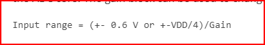
RESP= Bypass, RESN= Bypass, GAIN= 4, REFSEL= Internal reference( 0.6V), TACQ= 10us, MODE= SE, BURST= Disabled
If we feed 1.8V to AIN2 pin, the voltage for converting becomes 7.2V( 1.8V x 4).
Question 1) Is it harmful to nRF52832 due to the high voltage, 7.2V, for ADC conversion?
Question 2) What is the maximum voltage feed to AIN2 for ADC conversion if GAIN set to 4?