This post is older than 2 years and might not be relevant anymore
More Info: Consider searching for newer posts

NRF8001 problem

Hello!

I have Adafruit evaluation board with NRF8001 module and it works perfect.

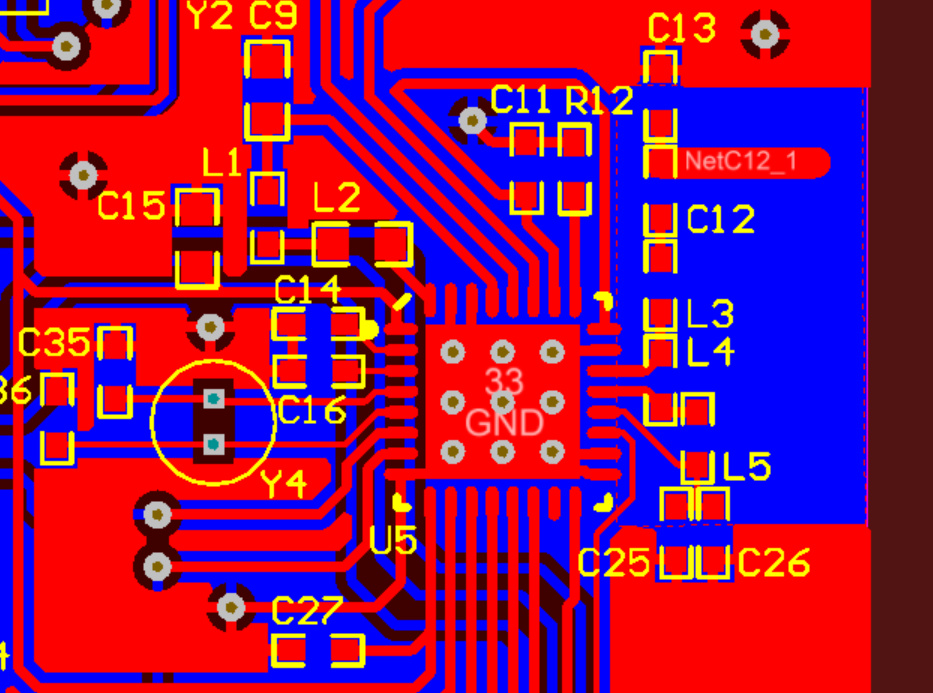
I also tried to develop my own board with microcontroller unit and NRF 8001 module, but device can't be found by other devices. I use NRF Master Control Application for Android. It successfully finds Adafruit board, but doesn't find my board. I use PCB antenna. PCB layout looks so:

image description

Schematic:

image description

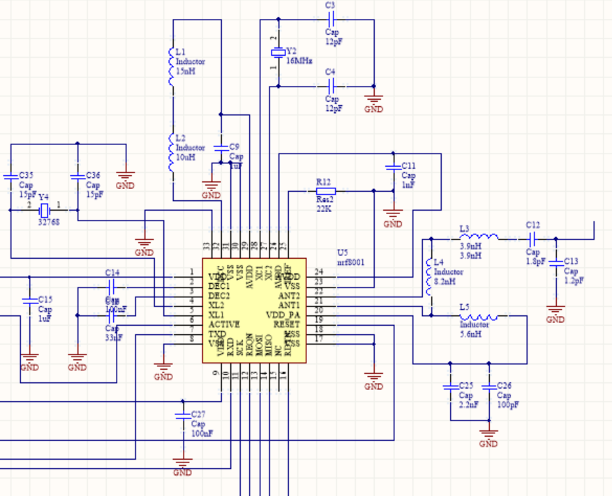
All ACI commands work correct both for Adafruit board and my own one. The only problem is that my board can't be found by the application. It seems like the problem is in my antenna, but both schematic and PCB layout are taken from tho Nordic examples. So I Can't understand where exactly the problem is.

Can you give me any advice please?

Thank you in advance.

  • Hi,

    The reference layout contains everything up to the 50 ohm transmission line between nRF chip and antenna. Antenna and antenna side tuning is not included. This means that both antenna and antenna matching network should be added, which seems to not be the case in your layout.

    For full designs including matching and antenna, see the Reference Designs. The nRF5x series are also 2.4 GHz BLE designs, so the antennas used in the nRF51 based reference designs can be used for 8001 as well.

    For tuning the antenna you can either rely on a single shunt capacitor and physically alter the antenna length, or you can use a pi network. If altering the antenna length, the antenna should be slightly longer in the prototype used for tuning, as physically cutting the antenna is relatively easy. Copying a tuned design from another project will not work, as the required matching depends on both the antenna the rest of the board. For more on antenna tuning, see the nWP017 - Antenna tuning whitepaper.

    What you should also do, is to make sure there are a lot of vias between the top and bottom ground layers. A well connected ground plane is super important. Also, remember not to have a ground layer around or below the antenna, as you can also see in the reference designs. A printed antenna starts where the ground plane ends. If using a chip antenna, the layout around the antenna must be identical to the reference layout in the datasheet for that particular antenna.

    Regards, Terje

  • Thank you very much! I'll try to follow your advices

Related