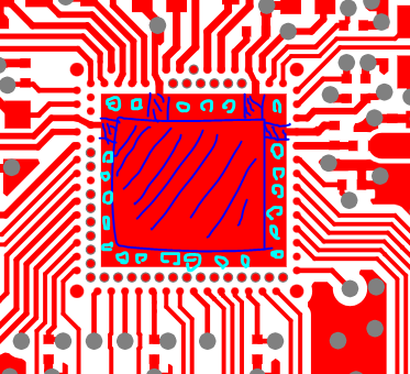
When I was considering the layout of the nRF5340 chip, I found that the pins of the nRF5340 chip are very small, and I need to punch the vias on the pads, and then use the process of plugging the holes and plating the copper layer in order to make sure that the solder won't flow inside the vias; however, this will incur high processing costs;
Therefore, I would like to ask if I can slightly reduce the size of the GND PAD in the middle, so that the pin lines of the inner ring can go out from the pad and then through the via to other layers, and then use the overlay soldermask layer to make sure that the via and the GND PAD on the chip won't be short-circuited, and in this way, reduce the cost of processing because of the directly punched holes on the pads;
What are the risks associated with this approach?Or is this practice not permitted?