
Hello everyone,
We are working on a low power design with a nrf52805. The low power feature did work well initially on the eval board.
When the main supply drops away we power the IC with a backup battery and go into low power mode until main power is back, then we reset the IC.
Now that we are integrating the design on the final PCB, the backup battery current consumption for the BLE part is higher than on a separate board.
The reason is that the BLE part on the PCB now shares its 3.3V supply with other components. When the main supply drops away, the nrf52805 is supplied by the backup battery.
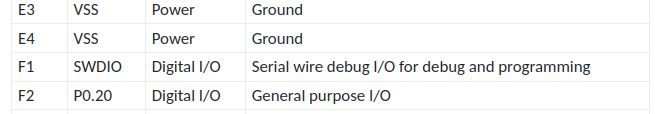
The debug IO's are protected by ESD protection tvs diodes. The nrf52805 SWDIO pin is still high in low power mode due to the internal Pull-up. Now the 3.3V of the SWDIO pin seem to deliver some current trough this tvs diodes to the 3.3V supply net of the rest of the PCB.
This does no harm in general, however, it shortens the lifespan of our backup battery by a lot.
Usually we are talking about some uA in low power mode. Now with the tvs diodes we are in the range of 1 -3 mA.
First thing we had in mind was to disable the SWDIO pin when we enter sleep mode. Then i did consult the pin specifications and noticed that SWDIO is not a general purpouse I/O.
Is it anyways possible to configure the SWDIO pin into an off state before we enter the sleep mode?
Thank you in advance, and best regards
Dino

