Via-in-pad recommendation for NRF52 – Need confirmation on manufacturer suggestion for resin-filled vias

Hello,

I am using the NRF52832 in my PCB design, and I have attached a screenshot of relevant part of the layout. My PCB manufacturer pointed out that some vias overlap with the pads of the NRF52 (in the center ground pad area), and they suggested filling these vias with resin to improve soldering reliability and prevent solder wicking during assembly.
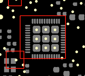
Before I proceed, I wanted to ask the following:

  1. Is resin-filled vias (via-in-pad) a common practice for NRF52-based designs?
  2. Are there any potential issues (thermal, mechanical, or electrical) specific to the NRF52 when using resin-filled vias in the ground pad region?
  3. Does Nordic have any specific recommendations regarding via treatment (like tenting, plugging, or filling) for the ground pad under the NRF52?
  4. Would this affect thermal performance or solder joint integrity in any way, considering the device's requirements?

Thanks in advance for your input!

Ron

  • Is resin-filled vias (via-in-pad) a common practice for NRF52-based designs?

    It's recommended for via in pad but not necessarily needed for the center pad. The vias will wick some of the solder so it depends on the diameter, length and number of vias plus the size of the paste mask aparture. If the amount of paste is large enough, you can tolerate that the vias wick some solder. But the easiest is of course to fill and plate the vias to avoid this. 

    Are there any potential issues (thermal, mechanical, or electrical) specific to the NRF52 when using resin-filled vias in the ground pad region?

    No, either ways are fine

    Does Nordic have any specific recommendations regarding via treatment (like tenting, plugging, or filling) for the ground pad under the NRF52?

    All designs, DKs and other, the last few years are using filled and tented vias. Pre nRF52 designs where using orinary vias in the center pads. For designs with nR52840 and other devices with the aQFN packet, one had to use via in the pad so filling and plating had to be done anyway. For QFN designs is more a question of the additional cost.

    Would this affect thermal performance or solder joint integrity in any way, considering the device's requirements?

    No 

Related