
Hello all,
I am designing a custom board utilizing the nRF52832 QFAA. For the first version of this board, I am attempting to closely replicate the layout of the nRF52832 QFAA in the nRF52832 dev kit. In doing so, I have been mocking our custom board after the schematic:
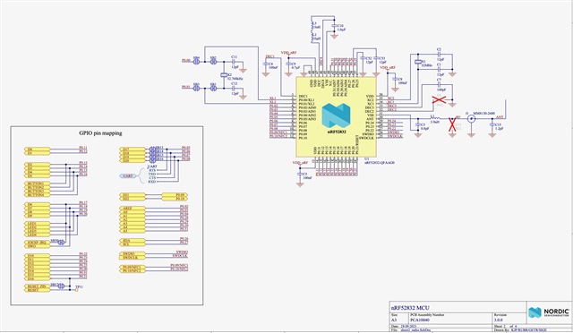
All has been intuitive except for the crossed out components (C6 and C13). Can someone explain how these two circuits should be configured? Should DEC2 just be NC or connected to ground (no decoupling capacitor)? Should C13 be removed, where L1 is the last component before J1?
Thanks!

