nRF5340 Breakout vias maximum size

Hello!

I'm using the nRF5340 for a school design project and as such am financially limited to relatively low cost board manufacturers.

It seems that most of these manufacturers only support through vias (no blind/buried) and have a minimum hole size larger than what is used in the nRF5340 DK. Right now I am looking at JLCPCB as they can also do turnkey assembly

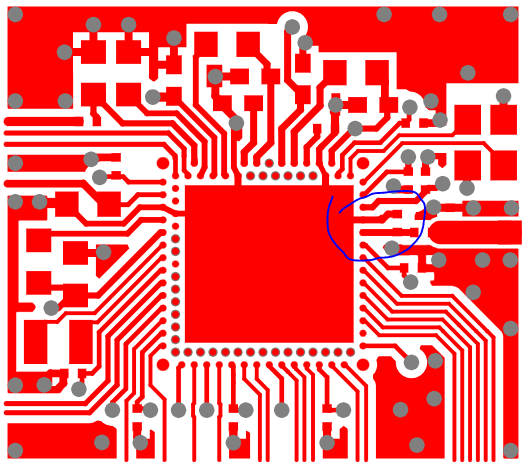
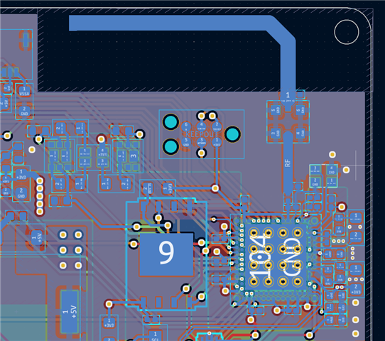
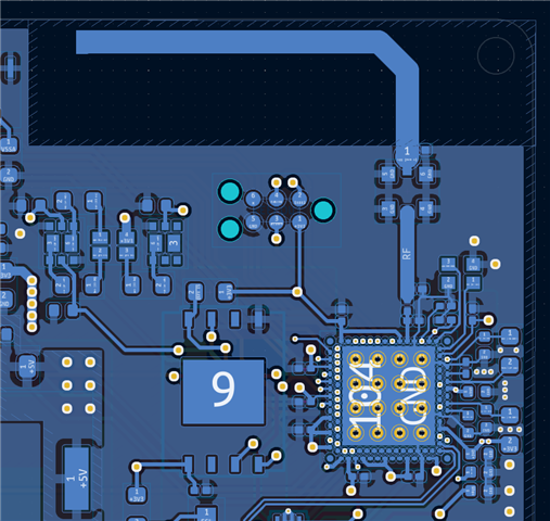
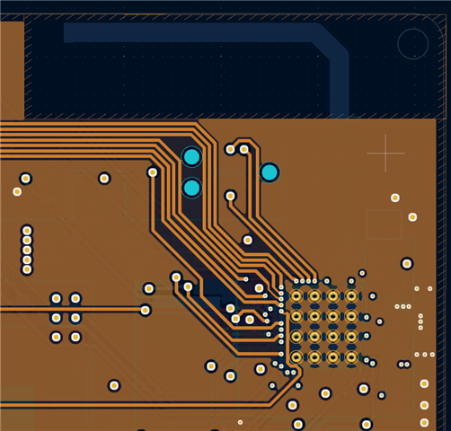
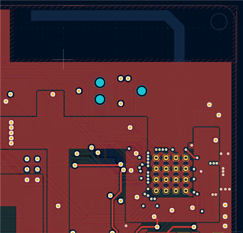
I mainly copied the layout from the DK, but have used the smallest vias I could for breaking out the inner pins and some of the outer ones. Current via specs are through vias with a hole size of 0.15mm and with a 0.3mm diameter. For reference the DK uses a 0.1mm hole size with 0.3mm diameter.

What are the odds that this hole size will work for connecting these pads? Screenshot of my current layout below (feel free to provide general layout criticism if there's anything of note, never worked on a project this dense before)

Images:

Any help would be very much appreciated!

  • Hi,


    Some general feedback first:


    For the RF section try to copy the ref design, if possible copy most of the layout. 


    We have a guide here: https://devzone.nordicsemi.com/guides/hardware-design-test-and-measuring/b/nrf5x/posts/general-pcb-design-guidelines-for-nrf53-series  


    I would also try to have a but more space between the connector and the tuning shunt cap for the antenna, this I just to make it easier to solder, the connector does take up some space and it can be tricky to gett the soldering iron close without touching the connector, and if it does, solderting can flow on to the connector and make it so it does not snapp properly on if there is some solder tin in the way. In addition it acts partially as a heatsink so more energy would be needed to get the solder to flow on the component pad. So a bit more space between these too makes things a easier.  


    As for the vias and the price concern. 
    Here are the reasons for why we use what we use:

    All our vias are capped or filled, this is because we dont want soldering to be sucked in to the hole, as this can result in poor soldering job and not enough contact. Can lead to poor connection and strange behavior in some cases. 

    For the size limitation, for the package variant that the nRF5340 uses the pins are small and the spacing is tight. This results in a limitations for manufacturing. Drilling such tiny holes through the PCB is difficult and most will not do it, so we use stacked vias instead. They are less expensive and can easily be caped\filled so solder flowing away is not an issue. They can also be very small. 

    We recommend to use via type 7 , https://resources.altium.com/p/IPC-vias, 

    I would try to avoid via in pad as much as possible and route the traces out from the pads a bit so that you can use through hole vias that are a bit bigger and cheaper. 


    So using via in pad for the pins here will likely result in some issues as it will increase the risk of some issues. 


    Try to talk to to the manufacturer her about what they think is best as well. 


    Here is an example on a partial solution we do on the dongle of the nRF5284:

    Two images show the same area, but you can see the vias that are placed close to the pads in areas circled with green. These vias are much bigger but we are able to fit them in there, but not one on each pin, so only a fe select pins are used. 


    Also want to add that the package type aQFN seems to produce some issues for the success rate from JLCPCB, they dont always successfully solder the SoC's in place so failure rate might be high. Contact them and ask to see what they can do for you, and also maybe try and contact another manufacturer, or prepare for some debugging. We some times see these productions fail with aQFN and the fix is often to re-solder og reflow the board. 


    Regards,
    Jonathan

Related