
Hello,
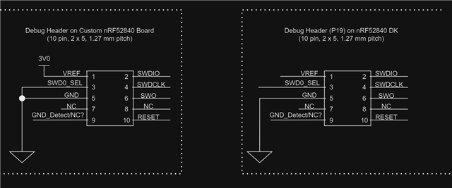
I'm designing a custom board with an nRF52840. I currently have an nRF52840 DK (PCA10056, v3.0.1) and would like to use the on-board debug out header (P19) to program/debug the nRF52840 on my custom board. I'm aware that the pinout for the debug header (P19) has changed from what is mentioned in the DK user guide. I've attached an image of how I plan to make my connections, I would appreciate it if someone could review them please.
Some addition context:
- I'm planning to power my custom board using a CR2032 coin cell battery (3.0V)
- I intend to use a 10 pin, 2 x 5, Socket-Socket, 1.27mm IDC cable (non-mirrored)
Q1) If I'm using the P19 debug out header, is SWD0_SEL supposed to be connected to GND or 3V0 on the custom board?
Q2) I don't want to power my custom board using the nRF52840 DK while programming/debugging it, is that okay? If so, am I supposed to short SB19 and connect VREF on pin1 which is 3V0 to VIO_REF and leave SB47 open (VDD isn't connected to VREF). I have attached an image below for reference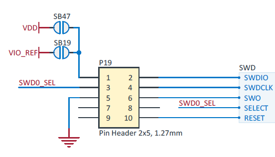
Q3) If SWD0_SEL has to be connected to GND on the custom board, would I also be able to use a J-Link Lite CortexM external debugger since the pinout would be the same. (TDI isn't used in SWD). I just wanna confirm and make sure I understand this properly. I have attached an image of the J-Link's debug header pinout below. 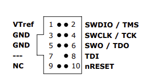
Thanks a ton in advance!
